SBAU171D May   2010  – January 2016 ADS1198 , ADS1298


  1.   ADS1298ECG-FE/ADS1198ECG-FE
    1.     Trademarks
    2. 1 ADS1298ECG-FE/ADS1198ECG-FE Overview
      1. 1.1 Important Disclaimer Information
      2. 1.2 Introduction
      3. 1.3 Supported Features
      4. 1.4 Features Not Supported in Current Version
      5. 1.5 ADS1x98ECG-FE Hardware
      6. 1.6 Minimum System Requirements for ADS1x98ECG-FE Evaluation Software
    3. 2 Quick Start
      1. 2.1 Default Jumper/Switch Configuration
      2. 2.2 ADS1x98ECG-FE Operation
    4. 3 Using the ADS1298ECG-FE Software
      1. 3.1 Application User Menu
      2. 3.2 Top-Level Application Controls
      3. 3.3 About Tab
      4. 3.4 ADC Register Tab
        1. 3.4.1 Standby and Reset Controls
        2. 3.4.2 Channel Registers Tab (ADC Register)
          1. 3.4.2.1 Global Channel Registers
          2. 3.4.2.2 Channel Control Registers
        3. 3.4.3 LOFF and RLD Tab (ADC Register)
          1. 3.4.3.1 Lead-Off Detection and Current Direction Control Registers
          2. 3.4.3.2 Right Leg Drive Derivation Control Registers
        4. 3.4.4 GPIO and OTHER Registers Tab (ADC Register)
          1. 3.4.4.1 Wilson Central and Augmented Lead Registers
        5. 3.4.5 Register Map (ADC Register)
      5. 3.5 Analysis Tab
        1. 3.5.1 Scope Tab (Anaysis)
          1. 3.5.1.1 Zoom Tool
        2. 3.5.2 Histogram Tab (Analysis)
        3. 3.5.3 FFT Tab
        4. 3.5.4 ECG Tab (Analysis)
      6. 3.6 Save Tab
    5. 4 ADS1x98ECG-FE Input Signals
      1. 4.1 Input Short Testing
      2. 4.2 Internal Test Signals Input
      3. 4.3 Temperature Sensor
      4. 4.4 Normal Electrode Input
        1. 4.4.1 Capturing 12-Lead ECG Signals
      5. 4.5 MVDD Input, RLD Measurement, RLD Positive Electrode Driver, and RLD Negative Electrode Driver
      6. 4.6 Lead Derivation
      7. 4.7 Wilson Center Terminal (WCT)
      8. 4.8 Right Leg Drive
        1. 4.8.1 RLD Common Mode Voltage
        2. 4.8.2 Driving the RLD Cable Shield
      9. 4.9 PACE Detection
    6. 5 ADS1298ECG-FE/ADS1198ECG-FE Hardware Details
      1. 5.1 Jumper Description
      2. 5.2 Power Supply
      3. 5.3 Clock
      4. 5.4 Reference
      5. 5.5 Analog Output Signals
      6. 5.6 Digital Signals
      7. 5.7 Analog Input Signals
        1. 5.7.1 Patient Simulator Input
        2. 5.7.2 Arbitrary Input Signals
  2. ASchematics, BOM, Layout, and ECG Cable Details
    1. A.1 Overview
    2. A.2 ADS1x98ECG-FE Front-End Board Schematics
    3. A.3 Bill of Materials
      1. Table 13. Bill of Materials: ADS1x98ECG-FE
    4. A.4 Printed Circuit Board Layout
    5. A.5 ECG Cable Details
  3. BExternal Optional Hardware
    1. B.1 Optional External Hardware (Not Included)
    2. B.2 ADS1x98ECG-FE Power-Supply Recommendations
  4. CSoftware Installation
    1. C.1 Minimum Requirements
    2. C.2 Installing the Software

ADS1x98ECG-FE Power-Supply Recommendations

If you chose to power the MMB0 board through the wall adapter jack, it must comply with the following requirements:

  • Output voltage: 5.5 VDC to 15 VDC
  • Maximum output current: 500 mA
  • Output connector: barrel plug (positive center), 2.5-mm I.D. x 5.5-mm O.D. (9-mm insertion depth)
  • Complies with applicable regional safety standards

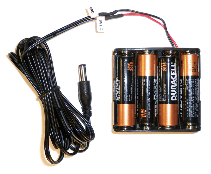
Figure 49 shows a +6V power-supply cable (not provided in the EVM kit) connected to a battery pack with four 1.5V batteries connected in series. Connecting to a wall-powered source makes the ADS1x98ECG-FE more susceptible to 50Hz/60Hz noise pickup; therefore, for best performance, it is recommended to power the ADS1x98ECG-FE with a battery source. This configuration minimizes the amount of noise pickup seen at the digitized output of the ADS1298.
hdwe_bat_pack_bau171.pngFigure 49. Recommended Power Supply for ADS1x98ECG-FE