ZHCSLD2E may 2020 – july 2023 UCC28782
PRODUCTION DATA
- 1
- 1 特性
- 2 应用
- 3 描述
- 4 Revision History
- 5 Device Comparison Table
- 6 Pin Configuration and Functions
- 7 Specifications
-
8 Detailed Description
- 8.1 Overview
- 8.2 Functional Block Diagram
- 8.3
Detailed Pin Description
- 8.3.1 BUR Pin (Programmable Burst Mode)
- 8.3.2 FB Pin (Feedback Pin)
- 8.3.3 REF Pin (Internal 5-V Bias)
- 8.3.4 VDD Pin (Device Bias Supply)
- 8.3.5 P13 and SWS Pins
- 8.3.6 S13 Pin
- 8.3.7 IPC Pin (Intelligent Power Control Pin)
- 8.3.8 RUN Pin (Driver and Bias Source for Isolator)
- 8.3.9 PWMH and AGND Pins
- 8.3.10 PWML and PGND Pins
- 8.3.11 SET Pin
- 8.3.12 RTZ Pin (Sets Delay for Transition Time to Zero)
- 8.3.13 RDM Pin (Sets Synthesized Demagnetization Time for ZVS Tuning)
- 8.3.14 BIN, BSW, and BGND Pins
- 8.3.15 XCD Pin
- 8.3.16 CS, VS, and FLT Pins
- 8.4
Device Functional Modes
- 8.4.1 Adaptive ZVS Control with Auto-Tuning
- 8.4.2 Dead-Time Optimization
- 8.4.3 EMI Dither and Dither Fading Function
- 8.4.4 Control Law across Entire Load Range
- 8.4.5 Adaptive Amplitude Modulation (AAM)
- 8.4.6 Adaptive Burst Mode (ABM)
- 8.4.7 Low Power Mode (LPM)
- 8.4.8 First Standby Power Mode (SBP1)
- 8.4.9 Second Standby Power Mode (SBP2)
- 8.4.10 Startup Sequence
- 8.4.11 Survival Mode of VDD (INT_STOP)
- 8.4.12 Capacitor Voltage Balancing Function
- 8.4.13 Device Functional Modes for Bias Regulator Control
- 8.4.14
System Fault Protections
- 8.4.14.1 Brown-In and Brown-Out
- 8.4.14.2 Output Over-Voltage Protection (OVP)
- 8.4.14.3 Input Over Voltage Protection (IOVP)
- 8.4.14.4 Over-Temperature Protection (OTP) on FLT Pin
- 8.4.14.5 Over-Temperature Protection (OTP) on CS Pin
- 8.4.14.6 Programmable Over-Power Protection (OPP)
- 8.4.14.7 Peak Power Limit (PPL)
- 8.4.14.8 Output Short-Circuit Protection (SCP)
- 8.4.14.9 Over-Current Protection (OCP)
- 8.4.14.10 External Shutdown
- 8.4.14.11 Internal Thermal Shutdown
- 8.4.15 Pin Open/Short Protections
-
9 Application and Implementation
- 9.1 Application Information
- 9.2
Typical Application Circuit
- 9.2.1 Design Requirements for a 65-W USB-PD Adapter Application
- 9.2.2
Detailed Design Procedure
- 9.2.2.1 Input Bulk Capacitance and Minimum Bulk Voltage
- 9.2.2.2 Transformer Calculations
- 9.2.2.3 Clamp Capacitor Calculation
- 9.2.2.4 Bleed-Resistor Calculation
- 9.2.2.5 Output Filter Calculation
- 9.2.2.6 Calculation of ZVS Sensing Network
- 9.2.2.7 Calculation of BUR Pin Resistances
- 9.2.2.8 Calculation of Compensation Network
- 9.2.3 Application Curves
- 10Power Supply Recommendations
- 11Layout
- 12Device and Documentation Support
- 13Mechanical, Packaging, and Orderable Information
8.3.5 P13 and SWS Pins
The P13 pin provides a regulated voltage to the gate of the depletion-mode MOSFET (QS), enabling QS to serve both VVDD start-up and loss-less ZVS-sensing from the high-voltage switch node (VSW) through the SWS pin. During VVDD start-up, the UVLO circuit controls two power-path switches connecting SWS and P13 pins to VDD pin with two internal current-limit resistors (RDDS and RDDH), as shown in Figure 8-5. In this configuration, QS behaves as a current source to charge the VDD capacitor (CVDD). RDDS is set at 5 kΩ when VVDD < 1.8 V to limit the maximum fault current under a VDD short-to-GND condition. RDDS is reduced to 500 Ω when VVDD > 1.8 V to allow VVDD to charge faster. The maximum charge current (ISWS) is affected by RDDS, the external series resistance (RSWS) from SWS pin to QS, and the threshold voltage of QS (VTH(Qs)). ISWS can be calculated as
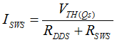
 Figure 8-5 Operation of the VDD Startup Circuit
After VVDD reaches VVDD(ON), the two power-path switches open the connections between SWS, P13, and VDD pins. At this point, a third power-path switch connects an internal 13-V regulator to the P13 pin for configuring QS to perform loss-less ZVS sensing. Since QS gate is fixed at 13 V, when the drain pin voltage of QS becomes higher than the sum of QS threshold voltage (VTH(Qs)) and the 13-V gate voltage, QS turns off and the source pin voltage of QS can no longer follow the drain pin voltage change. This gate control method makes QS act as a high-voltage blocking device with the drain pin connected to VSW. When the controller is switching, whenever VSW is lower than 13 V, QS turns on and forces the source pin voltage to follow VSW, becoming a replica of the VSW waveform at the lower voltage level, as illustrated in Figure 8-6.
The limited window for monitoring the VSW waveform is sufficient for ZVS control of the UCC28782, since the ZVS tuning threshold (VTH(SWS)) is set at 8.5 V for VSET = 5 V and set at 4 V for VSET = 0 V. The 8.5-V threshold is the auto-tuning target of the internal adaptive ZVS control loop for realizing a partial-ZVS condition on an ACF using Si primary switches. On the other hand, performing full ZVS operation is more suitable for an ACF with GaN primary switches. Using a 4-V threshold helps to compensate for sensing delay between VSW and the SWS pin.
The internal 13-V regulator requires a high-quality ceramic by-pass capacitor (CP13) between the P13 pin and AGND pin for noise filtering and providing compensation to the P13 regulator. The minimum CP13 value is 1 μF and an X7R-type dielectric capacitor with 25-V rating or better is recommended. The controller enters a fault state if the P13 pin is open or shorted to AGND during VVDD start-up, or if VP13 overshoot is higher than VP13(OV) of 15 V in run state. The output short-circuit current of P13 regulator (IP13(MAX)) is self-limited to approximately 130 mA.
During AAM and ABM if the negative magnetizing current is large enough, a low-side GaN device may operate in the reverse conduction condition before it turns on each switching cycle, so VSW may be around -5 V for a brief inteval and it appears on the SWS pin. The SWS-pin design of UCC28782 can sustain -6 V (continuous) and -10 V (transient) stress to enhance the robust operation of the GaN ACF power stage.
During this interval, QS is in the on-state and its body diode may conduct for a short time when the voltage drop across the on-state resistance of QS is high enough. The external RSWS can limit the forward current flowing through the QS body diode, so the reverse recovery charge of the body diode can be significantly reduced. Too high of RSWS value weakens the start-up charge current of CVDD and results in a longer start-up time. RSWS should be slightly higher than 500 Ω. A small back-to-back TVS across BSS126 gate-to-source should be added to protect the gate-to-source voltage from potential abnormal voltage stress. The TVS clamping voltage should be less than the BSS126 gate-to-source voltage rating but should not conduct below 15 V.
RSWS and a ceramic capacitor (CSWS) between the SWS pin and the bulk input capacitor ground form a small sensing delay to help the internal detection circuit to identify the ZVS characteristic correctly. The delay is to ensure that the ZCD detection on the VS pin happens earlier than the ZVS detection on the SWS pin, such that the ZVS control can auto-tune the PWMH on-time in the proper direction. The minimum value of CSWS is 22 pF.
 Figure 8-6 ZVS Sensing by Reusing the VDD Startup Circuit