ZHCSLD2E may 2020 – july 2023 UCC28782
PRODUCTION DATA
- 1
- 1 特性
- 2 应用
- 3 描述
- 4 Revision History
- 5 Device Comparison Table
- 6 Pin Configuration and Functions
- 7 Specifications
-
8 Detailed Description
- 8.1 Overview
- 8.2 Functional Block Diagram
- 8.3
Detailed Pin Description
- 8.3.1 BUR Pin (Programmable Burst Mode)
- 8.3.2 FB Pin (Feedback Pin)
- 8.3.3 REF Pin (Internal 5-V Bias)
- 8.3.4 VDD Pin (Device Bias Supply)
- 8.3.5 P13 and SWS Pins
- 8.3.6 S13 Pin
- 8.3.7 IPC Pin (Intelligent Power Control Pin)
- 8.3.8 RUN Pin (Driver and Bias Source for Isolator)
- 8.3.9 PWMH and AGND Pins
- 8.3.10 PWML and PGND Pins
- 8.3.11 SET Pin
- 8.3.12 RTZ Pin (Sets Delay for Transition Time to Zero)
- 8.3.13 RDM Pin (Sets Synthesized Demagnetization Time for ZVS Tuning)
- 8.3.14 BIN, BSW, and BGND Pins
- 8.3.15 XCD Pin
- 8.3.16 CS, VS, and FLT Pins
- 8.4
Device Functional Modes
- 8.4.1 Adaptive ZVS Control with Auto-Tuning
- 8.4.2 Dead-Time Optimization
- 8.4.3 EMI Dither and Dither Fading Function
- 8.4.4 Control Law across Entire Load Range
- 8.4.5 Adaptive Amplitude Modulation (AAM)
- 8.4.6 Adaptive Burst Mode (ABM)
- 8.4.7 Low Power Mode (LPM)
- 8.4.8 First Standby Power Mode (SBP1)
- 8.4.9 Second Standby Power Mode (SBP2)
- 8.4.10 Startup Sequence
- 8.4.11 Survival Mode of VDD (INT_STOP)
- 8.4.12 Capacitor Voltage Balancing Function
- 8.4.13 Device Functional Modes for Bias Regulator Control
- 8.4.14
System Fault Protections
- 8.4.14.1 Brown-In and Brown-Out
- 8.4.14.2 Output Over-Voltage Protection (OVP)
- 8.4.14.3 Input Over Voltage Protection (IOVP)
- 8.4.14.4 Over-Temperature Protection (OTP) on FLT Pin
- 8.4.14.5 Over-Temperature Protection (OTP) on CS Pin
- 8.4.14.6 Programmable Over-Power Protection (OPP)
- 8.4.14.7 Peak Power Limit (PPL)
- 8.4.14.8 Output Short-Circuit Protection (SCP)
- 8.4.14.9 Over-Current Protection (OCP)
- 8.4.14.10 External Shutdown
- 8.4.14.11 Internal Thermal Shutdown
- 8.4.15 Pin Open/Short Protections
-
9 Application and Implementation
- 9.1 Application Information
- 9.2
Typical Application Circuit
- 9.2.1 Design Requirements for a 65-W USB-PD Adapter Application
- 9.2.2
Detailed Design Procedure
- 9.2.2.1 Input Bulk Capacitance and Minimum Bulk Voltage
- 9.2.2.2 Transformer Calculations
- 9.2.2.3 Clamp Capacitor Calculation
- 9.2.2.4 Bleed-Resistor Calculation
- 9.2.2.5 Output Filter Calculation
- 9.2.2.6 Calculation of ZVS Sensing Network
- 9.2.2.7 Calculation of BUR Pin Resistances
- 9.2.2.8 Calculation of Compensation Network
- 9.2.3 Application Curves
- 10Power Supply Recommendations
- 11Layout
- 12Device and Documentation Support
- 13Mechanical, Packaging, and Orderable Information
8.4.13.1 Mitigation of Switching Interaction with ACF Converter
When the ACF control law is in AAM and ABM modes, the high side switch and ZVS control loop are enabled. In order to desensitize the boost switching noise interfering with the peak current loop and the ZVS control loop of the ACF converter, a unique switching misalignment function is activated for these two modes. When the ACF control law enters into LPM, SBP1, and SBP2 modes, the high side switch is disabled and the converter operates in valley switching, so switching misalignment function is disabled.
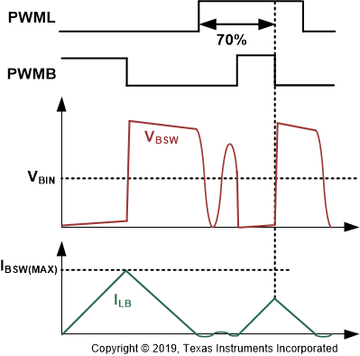
Since the bias regulator switch (QBSW) turns off at the highest peak current of the boost inductor, the lumped parasitic inductance from the BGND-pin bond wire and the PCB traces may create a voltage disturbance on the current sense signal, and might potentially result in prematurely turn-off of the PWML signal. When the PWML on time is disturbed, the ZVS control loop may introduce a small calculation error in the PWMH on time, so the ZVS switching may not be maintained for all switching cycles. To resolve this effect in UCC28782, the switching misalignment function will automatically avoid the intersection between the QBSW turn off edge and the PWML turn off edge to mitigate the noise interference. Specifically, if QBSW still stays in the on-state when the PWML signal reaches 70% on time, QBSW will be forced to be turned off earlier, so that the turn off instant for both the boost converter and ACF converter will not be aligned. Therefore, it is normal that the peak current of the boost inductor may not be consistent in AAM and ABM because of this misalignment function.
 Figure 8-35 Switching Misalignment Function
Besides the above di/dt coupling effect, both the dV/dt coupling through the parasitic capacitance of the boost switching node on the BSW pin and the dB/dt coupling through the inductor flux change need to be considered in the design. It is important that the noise-sensitive traces or components must be kept away from the high dV/dt BSW node and the high dB/dt boost inductor flux loop in order to minimize the coupling. A shielded chip ferrite inductor or a powder core chip inductor is preferred to minimize the flux coupling. If a non-shielding chip ferrite inductor has to be used, the inductor must not be close to the noise-sensitive components and controller pins.