ZHCSLD2E may 2020 – july 2023 UCC28782
PRODUCTION DATA
- 1
- 1 特性
- 2 应用
- 3 描述
- 4 Revision History
- 5 Device Comparison Table
- 6 Pin Configuration and Functions
- 7 Specifications
-
8 Detailed Description
- 8.1 Overview
- 8.2 Functional Block Diagram
- 8.3
Detailed Pin Description
- 8.3.1 BUR Pin (Programmable Burst Mode)
- 8.3.2 FB Pin (Feedback Pin)
- 8.3.3 REF Pin (Internal 5-V Bias)
- 8.3.4 VDD Pin (Device Bias Supply)
- 8.3.5 P13 and SWS Pins
- 8.3.6 S13 Pin
- 8.3.7 IPC Pin (Intelligent Power Control Pin)
- 8.3.8 RUN Pin (Driver and Bias Source for Isolator)
- 8.3.9 PWMH and AGND Pins
- 8.3.10 PWML and PGND Pins
- 8.3.11 SET Pin
- 8.3.12 RTZ Pin (Sets Delay for Transition Time to Zero)
- 8.3.13 RDM Pin (Sets Synthesized Demagnetization Time for ZVS Tuning)
- 8.3.14 BIN, BSW, and BGND Pins
- 8.3.15 XCD Pin
- 8.3.16 CS, VS, and FLT Pins
- 8.4
Device Functional Modes
- 8.4.1 Adaptive ZVS Control with Auto-Tuning
- 8.4.2 Dead-Time Optimization
- 8.4.3 EMI Dither and Dither Fading Function
- 8.4.4 Control Law across Entire Load Range
- 8.4.5 Adaptive Amplitude Modulation (AAM)
- 8.4.6 Adaptive Burst Mode (ABM)
- 8.4.7 Low Power Mode (LPM)
- 8.4.8 First Standby Power Mode (SBP1)
- 8.4.9 Second Standby Power Mode (SBP2)
- 8.4.10 Startup Sequence
- 8.4.11 Survival Mode of VDD (INT_STOP)
- 8.4.12 Capacitor Voltage Balancing Function
- 8.4.13 Device Functional Modes for Bias Regulator Control
- 8.4.14
System Fault Protections
- 8.4.14.1 Brown-In and Brown-Out
- 8.4.14.2 Output Over-Voltage Protection (OVP)
- 8.4.14.3 Input Over Voltage Protection (IOVP)
- 8.4.14.4 Over-Temperature Protection (OTP) on FLT Pin
- 8.4.14.5 Over-Temperature Protection (OTP) on CS Pin
- 8.4.14.6 Programmable Over-Power Protection (OPP)
- 8.4.14.7 Peak Power Limit (PPL)
- 8.4.14.8 Output Short-Circuit Protection (SCP)
- 8.4.14.9 Over-Current Protection (OCP)
- 8.4.14.10 External Shutdown
- 8.4.14.11 Internal Thermal Shutdown
- 8.4.15 Pin Open/Short Protections
-
9 Application and Implementation
- 9.1 Application Information
- 9.2
Typical Application Circuit
- 9.2.1 Design Requirements for a 65-W USB-PD Adapter Application
- 9.2.2
Detailed Design Procedure
- 9.2.2.1 Input Bulk Capacitance and Minimum Bulk Voltage
- 9.2.2.2 Transformer Calculations
- 9.2.2.3 Clamp Capacitor Calculation
- 9.2.2.4 Bleed-Resistor Calculation
- 9.2.2.5 Output Filter Calculation
- 9.2.2.6 Calculation of ZVS Sensing Network
- 9.2.2.7 Calculation of BUR Pin Resistances
- 9.2.2.8 Calculation of Compensation Network
- 9.2.3 Application Curves
- 10Power Supply Recommendations
- 11Layout
- 12Device and Documentation Support
- 13Mechanical, Packaging, and Orderable Information
9.2.2.7 Calculation of BUR Pin Resistances
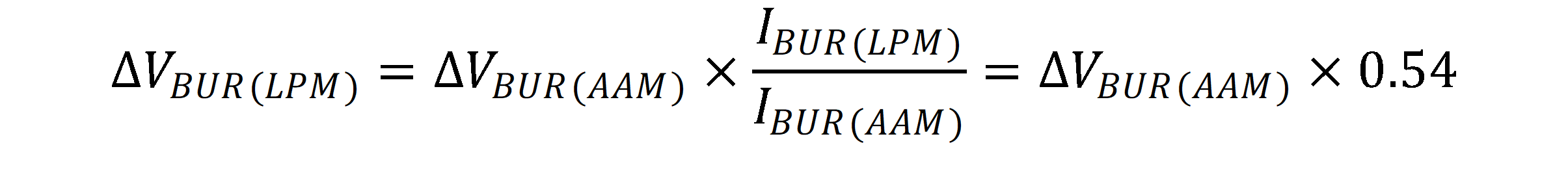
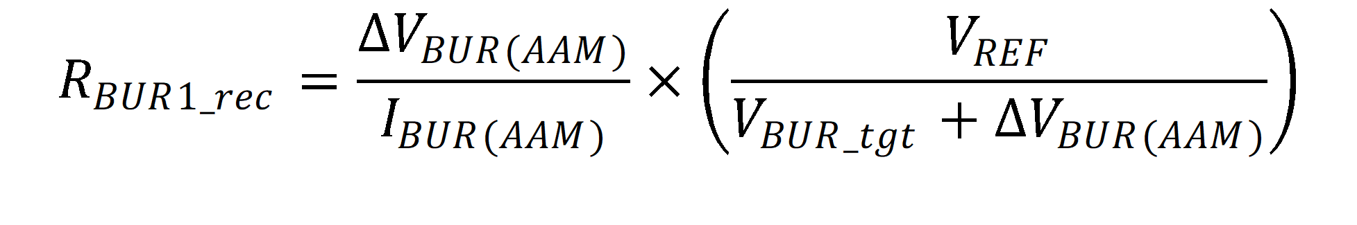
Referring back to Section 8.3.1, it is recommended that ABM is entered at no higher than 50% to 60% of full load. Equation 1 and Equation 2, or Equation 1 and Equation 4, provide two equations for calculating two unknowns for the BUR-pin resistor values. However, first the target values of VCST(BUR), ΔVBUR(AAM), and ΔVBUR(LPM) must be chosen. Since the ratio of IBUR(AAM) to IBUR(LPM) is fixed at 1.852 (5 µA / 2.7 µA), it is necessary to target ΔVBUR(AAM) = 185 mV to ensure that ΔVBUR(LPM) = 100 mV, per guidance in Section 8.3.1.
The procedure to determine the value of VCST(BUR) is quite complex and is not provided in this datasheet. Instead, the UCC28782 Excel Calculator Tool automatically calculates this value based on user input and determines the VBUR target voltage VBUR_tgt. Using this target value, it further determines the appropriate values for RBUR2 and RBUR1 to meet the BUR pin targets based on user selections for the following set of equations. Note that expected values are used to determine recommended resistances, then actual resistances are selected from standard value series and the resulting actual voltages are calculated from the selected resistor values. Actual voltage results should be close to the targeted values.
Calculate expected ΔVBUR(LPM) value based on ΔVBUR(AAM) target value.
Calculate the expected value for the parallel combination of RBUR1 with RBUR2.

Calculate the recommended value for RBUR1 and choose a standard 1% tolerance value for RBUR1_act that is close to the recommended value.
Calculate the recommended value for RBUR2 using RBUR1_act and choose a standard 1% tolerance value for RBUR2_act that is close to the recommended value.

Calculate the actual values for VBUR, ΔVBUR(AAM), and ΔVBUR(LPM) using RBUR1_act and RBUR2_act.


Finally, verify that the total summation of the BUR voltage with hysteresis does not exceed the BUR-pin upper clamp voltage of 2.4 V.