ZHCSLD2E may 2020 – july 2023 UCC28782
PRODUCTION DATA
- 1
- 1 特性
- 2 应用
- 3 描述
- 4 Revision History
- 5 Device Comparison Table
- 6 Pin Configuration and Functions
- 7 Specifications
-
8 Detailed Description
- 8.1 Overview
- 8.2 Functional Block Diagram
- 8.3
Detailed Pin Description
- 8.3.1 BUR Pin (Programmable Burst Mode)
- 8.3.2 FB Pin (Feedback Pin)
- 8.3.3 REF Pin (Internal 5-V Bias)
- 8.3.4 VDD Pin (Device Bias Supply)
- 8.3.5 P13 and SWS Pins
- 8.3.6 S13 Pin
- 8.3.7 IPC Pin (Intelligent Power Control Pin)
- 8.3.8 RUN Pin (Driver and Bias Source for Isolator)
- 8.3.9 PWMH and AGND Pins
- 8.3.10 PWML and PGND Pins
- 8.3.11 SET Pin
- 8.3.12 RTZ Pin (Sets Delay for Transition Time to Zero)
- 8.3.13 RDM Pin (Sets Synthesized Demagnetization Time for ZVS Tuning)
- 8.3.14 BIN, BSW, and BGND Pins
- 8.3.15 XCD Pin
- 8.3.16 CS, VS, and FLT Pins
- 8.4
Device Functional Modes
- 8.4.1 Adaptive ZVS Control with Auto-Tuning
- 8.4.2 Dead-Time Optimization
- 8.4.3 EMI Dither and Dither Fading Function
- 8.4.4 Control Law across Entire Load Range
- 8.4.5 Adaptive Amplitude Modulation (AAM)
- 8.4.6 Adaptive Burst Mode (ABM)
- 8.4.7 Low Power Mode (LPM)
- 8.4.8 First Standby Power Mode (SBP1)
- 8.4.9 Second Standby Power Mode (SBP2)
- 8.4.10 Startup Sequence
- 8.4.11 Survival Mode of VDD (INT_STOP)
- 8.4.12 Capacitor Voltage Balancing Function
- 8.4.13 Device Functional Modes for Bias Regulator Control
- 8.4.14
System Fault Protections
- 8.4.14.1 Brown-In and Brown-Out
- 8.4.14.2 Output Over-Voltage Protection (OVP)
- 8.4.14.3 Input Over Voltage Protection (IOVP)
- 8.4.14.4 Over-Temperature Protection (OTP) on FLT Pin
- 8.4.14.5 Over-Temperature Protection (OTP) on CS Pin
- 8.4.14.6 Programmable Over-Power Protection (OPP)
- 8.4.14.7 Peak Power Limit (PPL)
- 8.4.14.8 Output Short-Circuit Protection (SCP)
- 8.4.14.9 Over-Current Protection (OCP)
- 8.4.14.10 External Shutdown
- 8.4.14.11 Internal Thermal Shutdown
- 8.4.15 Pin Open/Short Protections
-
9 Application and Implementation
- 9.1 Application Information
- 9.2
Typical Application Circuit
- 9.2.1 Design Requirements for a 65-W USB-PD Adapter Application
- 9.2.2
Detailed Design Procedure
- 9.2.2.1 Input Bulk Capacitance and Minimum Bulk Voltage
- 9.2.2.2 Transformer Calculations
- 9.2.2.3 Clamp Capacitor Calculation
- 9.2.2.4 Bleed-Resistor Calculation
- 9.2.2.5 Output Filter Calculation
- 9.2.2.6 Calculation of ZVS Sensing Network
- 9.2.2.7 Calculation of BUR Pin Resistances
- 9.2.2.8 Calculation of Compensation Network
- 9.2.3 Application Curves
- 10Power Supply Recommendations
- 11Layout
- 12Device and Documentation Support
- 13Mechanical, Packaging, and Orderable Information
9.2.2.2.1 Primary-to-Secondary Turns Ratio (NPS)
NPS is a ratio of primary winding turns to secondary winding turns and although each winding must have a whole number of turns, the ratio of the two is not required to be a whole number. The choice of NPS influences the design tradeoffs on the voltage ratings between primary and secondary switches, and the balance between the magnetic core and winding loss of the transformer, which are explained in detail as follows:
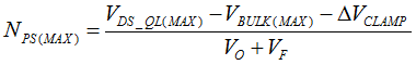
- Maximum NPS (NPS(MAX)) is limited by the maximum derated drain-to-source voltage of QL (VDS_QL(MAX)). In the expression below, ∆VCLAMP is a voltage deviation above the reflected output voltage. It can be either the ripple voltage of CCLAMP in AAM mode, or the voltage over-charge of CCLAMP by the leakage inductance energy when QH is disabled in LPM. VO is the output voltage, and VF is the forward voltage drop of the secondary rectifier.
Equation 27.
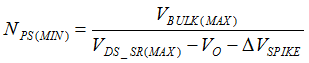
- Minimum NPS (NPS(MIN)) is limited by the maximum derated drain-to-source voltage of the secondary rectifier (VDS_SR(MAX)). In the expression for NPS(MIN), ∆VSPIKE should account for any additional voltage spike higher than VBULK(MAX)/NPS that occurs when QH is active and turns-off at non-zero current in AAM mode.
Equation 23.
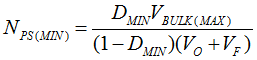
- Since the high-frequency transformer is usually a core-loss limited design instead of a saturation-limited design, the minimum duty cycle (DMIN) at VBULK(MAX) is more important. Lower DMIN increases core loss at VBULK(MAX), so this constraint creates another limitation on NPS(MIN).
Equation 24.
- The winding loss distribution between the primary and secondary side of the transformer is the final consideration. As NPS increases, primary RMS current reduces, while secondary RMS current increases. Conversely, as NPS decreases, primary RMS current increases, while secondary RMS current reduces.