ZHCSLD2E may 2020 – july 2023 UCC28782
PRODUCTION DATA
- 1
- 1 特性
- 2 应用
- 3 描述
- 4 Revision History
- 5 Device Comparison Table
- 6 Pin Configuration and Functions
- 7 Specifications
-
8 Detailed Description
- 8.1 Overview
- 8.2 Functional Block Diagram
- 8.3
Detailed Pin Description
- 8.3.1 BUR Pin (Programmable Burst Mode)
- 8.3.2 FB Pin (Feedback Pin)
- 8.3.3 REF Pin (Internal 5-V Bias)
- 8.3.4 VDD Pin (Device Bias Supply)
- 8.3.5 P13 and SWS Pins
- 8.3.6 S13 Pin
- 8.3.7 IPC Pin (Intelligent Power Control Pin)
- 8.3.8 RUN Pin (Driver and Bias Source for Isolator)
- 8.3.9 PWMH and AGND Pins
- 8.3.10 PWML and PGND Pins
- 8.3.11 SET Pin
- 8.3.12 RTZ Pin (Sets Delay for Transition Time to Zero)
- 8.3.13 RDM Pin (Sets Synthesized Demagnetization Time for ZVS Tuning)
- 8.3.14 BIN, BSW, and BGND Pins
- 8.3.15 XCD Pin
- 8.3.16 CS, VS, and FLT Pins
- 8.4
Device Functional Modes
- 8.4.1 Adaptive ZVS Control with Auto-Tuning
- 8.4.2 Dead-Time Optimization
- 8.4.3 EMI Dither and Dither Fading Function
- 8.4.4 Control Law across Entire Load Range
- 8.4.5 Adaptive Amplitude Modulation (AAM)
- 8.4.6 Adaptive Burst Mode (ABM)
- 8.4.7 Low Power Mode (LPM)
- 8.4.8 First Standby Power Mode (SBP1)
- 8.4.9 Second Standby Power Mode (SBP2)
- 8.4.10 Startup Sequence
- 8.4.11 Survival Mode of VDD (INT_STOP)
- 8.4.12 Capacitor Voltage Balancing Function
- 8.4.13 Device Functional Modes for Bias Regulator Control
- 8.4.14
System Fault Protections
- 8.4.14.1 Brown-In and Brown-Out
- 8.4.14.2 Output Over-Voltage Protection (OVP)
- 8.4.14.3 Input Over Voltage Protection (IOVP)
- 8.4.14.4 Over-Temperature Protection (OTP) on FLT Pin
- 8.4.14.5 Over-Temperature Protection (OTP) on CS Pin
- 8.4.14.6 Programmable Over-Power Protection (OPP)
- 8.4.14.7 Peak Power Limit (PPL)
- 8.4.14.8 Output Short-Circuit Protection (SCP)
- 8.4.14.9 Over-Current Protection (OCP)
- 8.4.14.10 External Shutdown
- 8.4.14.11 Internal Thermal Shutdown
- 8.4.15 Pin Open/Short Protections
-
9 Application and Implementation
- 9.1 Application Information
- 9.2
Typical Application Circuit
- 9.2.1 Design Requirements for a 65-W USB-PD Adapter Application
- 9.2.2
Detailed Design Procedure
- 9.2.2.1 Input Bulk Capacitance and Minimum Bulk Voltage
- 9.2.2.2 Transformer Calculations
- 9.2.2.3 Clamp Capacitor Calculation
- 9.2.2.4 Bleed-Resistor Calculation
- 9.2.2.5 Output Filter Calculation
- 9.2.2.6 Calculation of ZVS Sensing Network
- 9.2.2.7 Calculation of BUR Pin Resistances
- 9.2.2.8 Calculation of Compensation Network
- 9.2.3 Application Curves
- 10Power Supply Recommendations
- 11Layout
- 12Device and Documentation Support
- 13Mechanical, Packaging, and Orderable Information
8.3.14 BIN, BSW, and BGND Pins
A high-impedance resistor is integrated inside the BIN pin to sense the bias regulator input voltage and determine the regulator operating mode. A 30-V rated MOSFET (QBSW) with 1.4-Ω RDS(on) is integrated in the controller, whose drain is connected to the BSW pin and the source is to the BGND pin. When VBIN is less than the 2.2-V UVLO(ON) threshold (VBIN(ON)) and VVDD is still higher than the 13-V survival mode threshold (VVDD(PCT) + VVDD(OFF)), the regulator remains in the disabled condition. If the survival mode is triggered by VVDD < 13 V, QBSW is forced to switch regardless of VBIN < VBIN(ON) or not, and the regulator operates in continuous conduction mode (CCM) to charge CVDD quickly. If VVDD > 13 V, QBSW switching is enabled when VBIN > VBIN(ON) , and the regulator operates in transition mode or discontinuous conduction mode (DCM) to boost VVDD to the 18.5-V regulation level (VVDD(BOOST)). When the regulator starts switching, the 190-ns leading edge blanking time of QBSW is used to sample VBIN for under-voltage. If VBIN drops below the 1-V UVLO(OFF) threshold (VBIN(ON) - VBIN(OFF)), the regulator switching will be terminated immediately.
When the ACF output voltage increases and VBIN reaches to the 15-V boost disable threshold (VBIN(EN) + VBIN(DIS)), so the regulator will stop switching and VVDD is directly supplied from the rectified auxiliary winding voltage through the boost inductor and boost diode. When VBIN drops below the 14.8-V boost enable threshold (VBIN(EN)), the switching regulator will take over boosting of the VDD supply.
Two separate capacitors are recommended for the regulator input capacitor bank of the BIN pin. One is placed closer to the auxiliary winding and its rectification diode, so the switching loop of the primary auxiliary winding output can be minimized. A 33-µF chip ceramic capacitor is recommended for energy storage. The other capacitor is placed closer to the boost inductor, BSW, and BGND pins, so the regulator input switching loop can be reduced as well. A 10-µF chip ceramic capacitor is recommended for high-frequency decoupling. Ground return of the regulator output capacitor (CVDD) should be connected back to the BGND pin as close as possible in order to minimize the regulator output switching loop area. Rather than with the BGND pin, the low-noise ground terminal of CVDD should be used to connect the BGND net to the AGND pin with a low impedance copper trace or copper pour.
When the boost inductor current flowing through QBSW reaches to the 0.33-A peak current threshold, QBSW turns off in every boost switching cycle. A 30-V rated Schottky diode with higher than 0.4-A rated peak current capability is needed between the BSW and VDD pins in order to handle the 0.33-A switching current. The boost inductor between the BIN and BSW pins should support higher than 0.4-A saturation current capability. Higher current peaks may ring through the inductor whenever CBIN is charged higher than CVDD.
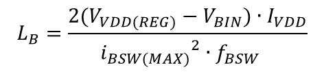
As the following equation shows, the inductance (LB) is determined based on the largest total supply current to the loading on the VDD pin and the highest boost switching frequency selection (fBSW), which is limited by maximum boost switching frequency (fBSW(MAX)) of the control loop. The minimum inductance is 22 µH (±10%) regardless of calculation result. Magnetic shielding is recommended to help avoid inducing noise into nearby networks.
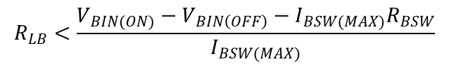
The voltage drop on the DC winding resistance of the boost inductor (RLB) and RDS(ON) of QBSW (RBSW) reduces the actual voltage across the boost inductance from VBIN. The boost inductor voltage needs to be high enough to build up the inductor current quickly. Therefore, it is recommended to choose the RLB low enough to make the total resistive voltage drop at 0.33 A lower than the 1-V boost UVLO(OFF) threshold.
When the ACF operates in the LPM, SBP1, and SBP2 modes, the high side switch is disabled, so the leakage inductance energy will charge the clamping capacitor and CBIN in every ACF switching cycle. If the leakage inductance energy is big enough to build up VBIN higher than 30 V under those operating modes, a unidirectional TVS between the BIN pin and AGND pin will be needed to protect the 30-V rated BIN and BSW pins. A high-voltage Schottky auxiliary winding rectifier diode maximizes the CBIN voltage in the survival mode, so the regulator in CCM mode can transfer the stored CBIN charge to CVDD. The more survival mode energy is absorbed by the auxiliary power supply, the less residual energy is delivered to the output capacitor. This will ensure that the output voltage can stay within regulation range during survival mode under no-load condition.