ZHCSLD2E may 2020 – july 2023 UCC28782
PRODUCTION DATA
- 1
- 1 特性
- 2 应用
- 3 描述
- 4 Revision History
- 5 Device Comparison Table
- 6 Pin Configuration and Functions
- 7 Specifications
-
8 Detailed Description
- 8.1 Overview
- 8.2 Functional Block Diagram
- 8.3
Detailed Pin Description
- 8.3.1 BUR Pin (Programmable Burst Mode)
- 8.3.2 FB Pin (Feedback Pin)
- 8.3.3 REF Pin (Internal 5-V Bias)
- 8.3.4 VDD Pin (Device Bias Supply)
- 8.3.5 P13 and SWS Pins
- 8.3.6 S13 Pin
- 8.3.7 IPC Pin (Intelligent Power Control Pin)
- 8.3.8 RUN Pin (Driver and Bias Source for Isolator)
- 8.3.9 PWMH and AGND Pins
- 8.3.10 PWML and PGND Pins
- 8.3.11 SET Pin
- 8.3.12 RTZ Pin (Sets Delay for Transition Time to Zero)
- 8.3.13 RDM Pin (Sets Synthesized Demagnetization Time for ZVS Tuning)
- 8.3.14 BIN, BSW, and BGND Pins
- 8.3.15 XCD Pin
- 8.3.16 CS, VS, and FLT Pins
- 8.4
Device Functional Modes
- 8.4.1 Adaptive ZVS Control with Auto-Tuning
- 8.4.2 Dead-Time Optimization
- 8.4.3 EMI Dither and Dither Fading Function
- 8.4.4 Control Law across Entire Load Range
- 8.4.5 Adaptive Amplitude Modulation (AAM)
- 8.4.6 Adaptive Burst Mode (ABM)
- 8.4.7 Low Power Mode (LPM)
- 8.4.8 First Standby Power Mode (SBP1)
- 8.4.9 Second Standby Power Mode (SBP2)
- 8.4.10 Startup Sequence
- 8.4.11 Survival Mode of VDD (INT_STOP)
- 8.4.12 Capacitor Voltage Balancing Function
- 8.4.13 Device Functional Modes for Bias Regulator Control
- 8.4.14
System Fault Protections
- 8.4.14.1 Brown-In and Brown-Out
- 8.4.14.2 Output Over-Voltage Protection (OVP)
- 8.4.14.3 Input Over Voltage Protection (IOVP)
- 8.4.14.4 Over-Temperature Protection (OTP) on FLT Pin
- 8.4.14.5 Over-Temperature Protection (OTP) on CS Pin
- 8.4.14.6 Programmable Over-Power Protection (OPP)
- 8.4.14.7 Peak Power Limit (PPL)
- 8.4.14.8 Output Short-Circuit Protection (SCP)
- 8.4.14.9 Over-Current Protection (OCP)
- 8.4.14.10 External Shutdown
- 8.4.14.11 Internal Thermal Shutdown
- 8.4.15 Pin Open/Short Protections
-
9 Application and Implementation
- 9.1 Application Information
- 9.2
Typical Application Circuit
- 9.2.1 Design Requirements for a 65-W USB-PD Adapter Application
- 9.2.2
Detailed Design Procedure
- 9.2.2.1 Input Bulk Capacitance and Minimum Bulk Voltage
- 9.2.2.2 Transformer Calculations
- 9.2.2.3 Clamp Capacitor Calculation
- 9.2.2.4 Bleed-Resistor Calculation
- 9.2.2.5 Output Filter Calculation
- 9.2.2.6 Calculation of ZVS Sensing Network
- 9.2.2.7 Calculation of BUR Pin Resistances
- 9.2.2.8 Calculation of Compensation Network
- 9.2.3 Application Curves
- 10Power Supply Recommendations
- 11Layout
- 12Device and Documentation Support
- 13Mechanical, Packaging, and Orderable Information
8.4.13 Device Functional Modes for Bias Regulator Control
When there is no overlapping between PWML on time and BSW on time and the survival mode is not triggered, there are two operating modes for the bias regulator when VBIN is between the UVLO(ON) threshold and the disable threshold. The first is the constant peak current (CPC) control mode for a heavier VDD load condition, and the second is the burst mode (BM) control for a light VDD load condition. The 18.5-V regulation in CPC is maintained by varying the boost switching frequency, and the peak current of the boost inductor is fixed at approx. 0.33 A. The 18.5-V regulation in BM is maintained by changing the burst frequency with a constant peak current for each switching cycle of a burst packet. There are at least 3 switching cycles in a burst packet for BM. E.g. when a 22-µH boost inductor (LB) is used, the mode transition point is at approx. 3-mA VDD load.
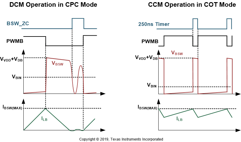
In CPC mode, the VVDD regulation is achieved by changing the boost switching frequency (fBSW) with a fixed 0.33-A peak current. When fBSW is reduced to the minimum controllable frequency, the control loop will automatically transition into BM. Figure 8-34 illustrates the switching pattern in CPC mode operating in the transition mode or discontinuous conduction mode (DCM). The internal ZCD detection on BSW pin only allows the turn on instant of the next boost switching cycle to happen after the BSW-pin voltage falls below the BIN-pin voltage, so that the boost inductor current drops to zero first.
 Figure 8-34 Switching Pattern of Boost Converter in CPC and COT Modes
If survival mode is enabled, the regulator will start switching regardless of VBIN level and enter into constant off time (COT) control mode. The COT control mode disables the ZCD detection on the BSW pin and creates a 250-ns off time in order to force the regulator into the continuous conduction mode (CCM). More energy per cycle can transfer from the BIN-pin capacitor to the VDD capacitor in CCM, so VVDD can be ramped up above the 13-V survival mode threshold faster than DCM, and minimize the survival mode energy transfer to the output capacitor on the ACF secondary side, as a result of the drop in VBIN. When VVDD is higher than 13 V, the regulator will automatically change the operation mode back to CPC or BM.
Besides survival mode, when the voltage difference between VVDD and VBIN is less than 1 V, the regulator will also disable ZCD detection and allows CCM operation. If ZCD is not disabled, the low voltage difference makes the demagnetization time of the boost inductor current very long, so VVDD would not be able to build up to the regulation level. The CCM operation can transfer the energy to VDD capacitor quickly, so VVDD can recover back to the regulation level.