ZHCSLD2E may 2020 – july 2023 UCC28782
PRODUCTION DATA
- 1
- 1 特性
- 2 应用
- 3 描述
- 4 Revision History
- 5 Device Comparison Table
- 6 Pin Configuration and Functions
- 7 Specifications
-
8 Detailed Description
- 8.1 Overview
- 8.2 Functional Block Diagram
- 8.3
Detailed Pin Description
- 8.3.1 BUR Pin (Programmable Burst Mode)
- 8.3.2 FB Pin (Feedback Pin)
- 8.3.3 REF Pin (Internal 5-V Bias)
- 8.3.4 VDD Pin (Device Bias Supply)
- 8.3.5 P13 and SWS Pins
- 8.3.6 S13 Pin
- 8.3.7 IPC Pin (Intelligent Power Control Pin)
- 8.3.8 RUN Pin (Driver and Bias Source for Isolator)
- 8.3.9 PWMH and AGND Pins
- 8.3.10 PWML and PGND Pins
- 8.3.11 SET Pin
- 8.3.12 RTZ Pin (Sets Delay for Transition Time to Zero)
- 8.3.13 RDM Pin (Sets Synthesized Demagnetization Time for ZVS Tuning)
- 8.3.14 BIN, BSW, and BGND Pins
- 8.3.15 XCD Pin
- 8.3.16 CS, VS, and FLT Pins
- 8.4
Device Functional Modes
- 8.4.1 Adaptive ZVS Control with Auto-Tuning
- 8.4.2 Dead-Time Optimization
- 8.4.3 EMI Dither and Dither Fading Function
- 8.4.4 Control Law across Entire Load Range
- 8.4.5 Adaptive Amplitude Modulation (AAM)
- 8.4.6 Adaptive Burst Mode (ABM)
- 8.4.7 Low Power Mode (LPM)
- 8.4.8 First Standby Power Mode (SBP1)
- 8.4.9 Second Standby Power Mode (SBP2)
- 8.4.10 Startup Sequence
- 8.4.11 Survival Mode of VDD (INT_STOP)
- 8.4.12 Capacitor Voltage Balancing Function
- 8.4.13 Device Functional Modes for Bias Regulator Control
- 8.4.14
System Fault Protections
- 8.4.14.1 Brown-In and Brown-Out
- 8.4.14.2 Output Over-Voltage Protection (OVP)
- 8.4.14.3 Input Over Voltage Protection (IOVP)
- 8.4.14.4 Over-Temperature Protection (OTP) on FLT Pin
- 8.4.14.5 Over-Temperature Protection (OTP) on CS Pin
- 8.4.14.6 Programmable Over-Power Protection (OPP)
- 8.4.14.7 Peak Power Limit (PPL)
- 8.4.14.8 Output Short-Circuit Protection (SCP)
- 8.4.14.9 Over-Current Protection (OCP)
- 8.4.14.10 External Shutdown
- 8.4.14.11 Internal Thermal Shutdown
- 8.4.15 Pin Open/Short Protections
-
9 Application and Implementation
- 9.1 Application Information
- 9.2
Typical Application Circuit
- 9.2.1 Design Requirements for a 65-W USB-PD Adapter Application
- 9.2.2
Detailed Design Procedure
- 9.2.2.1 Input Bulk Capacitance and Minimum Bulk Voltage
- 9.2.2.2 Transformer Calculations
- 9.2.2.3 Clamp Capacitor Calculation
- 9.2.2.4 Bleed-Resistor Calculation
- 9.2.2.5 Output Filter Calculation
- 9.2.2.6 Calculation of ZVS Sensing Network
- 9.2.2.7 Calculation of BUR Pin Resistances
- 9.2.2.8 Calculation of Compensation Network
- 9.2.3 Application Curves
- 10Power Supply Recommendations
- 11Layout
- 12Device and Documentation Support
- 13Mechanical, Packaging, and Orderable Information
8.3.1 BUR Pin (Programmable Burst Mode)
The voltage at the BUR pin (VBUR) sets a target peak current-sense threshold at the CS pin (VCST(BUR)) which programs the onset of adaptive burst mode (ABM). VBUR also determines the clamped peak current level of switching cycles in each burst packet. When VBUR is set higher, ABM will start at heavier output load conditions with higher peak primary current, so the benefit is higher light-load efficiency but the side effect is larger burst-mode output voltage ripple. Therefore, 50% to 60% of output load at high line is the recommended highest load condition to enter ABM (IO(BUR)) for both Si and GaN-based ACF designs.
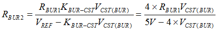
The relationship between VBUR and VCST(BUR) is a constant gain of KBUR-CST, so targeting VCST(BUR) just requires properly selecting the resistor divider on the BUR pin formed by RBUR1 and RBUR2. VBUR should be set between 0.7 V and 2.4 V, which constitute internal limits. If VBUR is less than 0.7 V, VCST(BUR) holds at 0.7 V / KBUR-CST. If VBUR is higher than 2.4 V, VCST(BUR) holds at 2.4 V / KBUR-CST. Targeting an excessively low or high percentage of load for entering ABM will engage one of these internal limits.
In order to enhance the mode transition between ABM and LPM, a programmable offset voltage (ΔVBUR(LPM)) is generated on top of the VBUR setting in ABM through an internal 2.7-μA current source (IBUR(LPM)), as shown in Figure 8-1. In ABM, VBUR is set through the resistor voltage divider to fulfill the target average efficiency. On transition from ABM to LPM, IBUR(LPM) is enabled in LPM and flows out of the BUR pin, so ΔVBUR(LPM) can be programmed based on the Thevenin resistance on the BUR pin, which can be expressed as
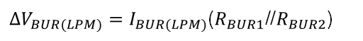
 Figure 8-1 Hysteresis Voltage Generation on BUR Pin
When VBUR steps higher on transition into LPM, the initial peak magnetizing current in LPM is increased with larger energy per switching cycle in each burst packet. This increases the output voltage which forces higher feedback current to restore regulation. Higher feedback current causes UCC28782 to stay in LPM, forming a hysteresis effect. If ΔVBUR(LPM) is designed too small, it is possible that mode toggling between LPM and ABM can occur resulting in audible noise. For that situation, ΔVBUR(LPM) greater than 100 mV is recommended.
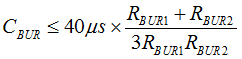
To minimize the effects of external noise coupling on VBUR, a filter capacitor on the BUR pin (CBUR) may be needed. CBUR needs to be properly designed to minimize the delay in generating ΔVBUR during mode transitions. It is recommended that CBUR should be sized small enough to ensure ΔVBUR(LPM) settles within 40 μs, corresponding to the burst frequency of 25 kHz in LPM (fLPM). Based on three RC time constants, representing 95% of a settled steady-state value from a step response, the design guide for CBUR is expressed as
In order to enhance the mode transition between ABM and AAM, a programmable offset voltage (ΔVBUR(AAM)) is generated to lower the VBUR with an internal 5-μA pull-down current (IBUR(AAM)), as shown in Figure 8-1. After transition from ABM to AAM, IBUR(AAM) is enabled in AAM and flows into the BUR pin, so ΔVBUR(AAM) is also programmed based on the Thevenin resistance on the BUR pin, which can be expressed as
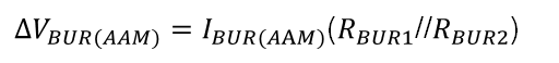
When VBUR reduces after transition to AAM, the initial peak magnetizing current in AAM is reduced with less energy per switching cycle, which forces UCC28782 to stay in AAM. If ΔVBUR(AAM) is too small, it is possible that either mode toggling between ABM and AAM or low-frequency ABM burst packets less than 20 kHz can occur and result in audible noise concern. For that situation, ΔVBUR(AAM) greater than 150 mV is recommended. In some power stage designs, LPM in hard switching condition may cover a wider output load current range, so the light-load efficiency in LPM may be lower than ABM with ZVS condition. Besides, the ABM-to-AAM mode transition may be affected potentially when the load current condition of LPM-to-ABM transition is too close to the load current condition of ABM-AAM transition.
In order to narrow down the output load current range in LPM, lower VBUR(ABM), smaller ΔVBUR(LPM), larger ROPP, and smaller CCS help to reduce the peak magnetizing current in LPM. If the LPM energy needs to be further reduced but VBUR in AAM is limited by the 0.7-V minimum programmable level, the optional application circuit in Figure 8-2 can be considered. When the output load current is reduced, duty cycle of each burst packet becomes smaller, so as the duty cycle of RUN-pin voltage. CBUR is discharged by the RUN driver through the small-signal diode (DBUR) and the current limit resistor (RRUN). Proper selection of RRUN value can further reduce VBUR(ABM) when the load current is reduced close to the transition point from ABM to LPM. One example BUR-pin setting is RBUR1 = 182 kΩ, RBUR2 = 37.4 kΩ, CBUR = 330 pF, and RRUN = 20 kΩ.
 Figure 8-2 Optional Application Circuit to Reduce VBUR in LPM