ZHCSLD2E may 2020 – july 2023 UCC28782
PRODUCTION DATA
- 1
- 1 特性
- 2 应用
- 3 描述
- 4 Revision History
- 5 Device Comparison Table
- 6 Pin Configuration and Functions
- 7 Specifications
-
8 Detailed Description
- 8.1 Overview
- 8.2 Functional Block Diagram
- 8.3
Detailed Pin Description
- 8.3.1 BUR Pin (Programmable Burst Mode)
- 8.3.2 FB Pin (Feedback Pin)
- 8.3.3 REF Pin (Internal 5-V Bias)
- 8.3.4 VDD Pin (Device Bias Supply)
- 8.3.5 P13 and SWS Pins
- 8.3.6 S13 Pin
- 8.3.7 IPC Pin (Intelligent Power Control Pin)
- 8.3.8 RUN Pin (Driver and Bias Source for Isolator)
- 8.3.9 PWMH and AGND Pins
- 8.3.10 PWML and PGND Pins
- 8.3.11 SET Pin
- 8.3.12 RTZ Pin (Sets Delay for Transition Time to Zero)
- 8.3.13 RDM Pin (Sets Synthesized Demagnetization Time for ZVS Tuning)
- 8.3.14 BIN, BSW, and BGND Pins
- 8.3.15 XCD Pin
- 8.3.16 CS, VS, and FLT Pins
- 8.4
Device Functional Modes
- 8.4.1 Adaptive ZVS Control with Auto-Tuning
- 8.4.2 Dead-Time Optimization
- 8.4.3 EMI Dither and Dither Fading Function
- 8.4.4 Control Law across Entire Load Range
- 8.4.5 Adaptive Amplitude Modulation (AAM)
- 8.4.6 Adaptive Burst Mode (ABM)
- 8.4.7 Low Power Mode (LPM)
- 8.4.8 First Standby Power Mode (SBP1)
- 8.4.9 Second Standby Power Mode (SBP2)
- 8.4.10 Startup Sequence
- 8.4.11 Survival Mode of VDD (INT_STOP)
- 8.4.12 Capacitor Voltage Balancing Function
- 8.4.13 Device Functional Modes for Bias Regulator Control
- 8.4.14
System Fault Protections
- 8.4.14.1 Brown-In and Brown-Out
- 8.4.14.2 Output Over-Voltage Protection (OVP)
- 8.4.14.3 Input Over Voltage Protection (IOVP)
- 8.4.14.4 Over-Temperature Protection (OTP) on FLT Pin
- 8.4.14.5 Over-Temperature Protection (OTP) on CS Pin
- 8.4.14.6 Programmable Over-Power Protection (OPP)
- 8.4.14.7 Peak Power Limit (PPL)
- 8.4.14.8 Output Short-Circuit Protection (SCP)
- 8.4.14.9 Over-Current Protection (OCP)
- 8.4.14.10 External Shutdown
- 8.4.14.11 Internal Thermal Shutdown
- 8.4.15 Pin Open/Short Protections
-
9 Application and Implementation
- 9.1 Application Information
- 9.2
Typical Application Circuit
- 9.2.1 Design Requirements for a 65-W USB-PD Adapter Application
- 9.2.2
Detailed Design Procedure
- 9.2.2.1 Input Bulk Capacitance and Minimum Bulk Voltage
- 9.2.2.2 Transformer Calculations
- 9.2.2.3 Clamp Capacitor Calculation
- 9.2.2.4 Bleed-Resistor Calculation
- 9.2.2.5 Output Filter Calculation
- 9.2.2.6 Calculation of ZVS Sensing Network
- 9.2.2.7 Calculation of BUR Pin Resistances
- 9.2.2.8 Calculation of Compensation Network
- 9.2.3 Application Curves
- 10Power Supply Recommendations
- 11Layout
- 12Device and Documentation Support
- 13Mechanical, Packaging, and Orderable Information
8.4.14.6 Programmable Over-Power Protection (OPP)
The over-power protection (OPP) allows operation in an over-power condition for a limited amount of time, so the UCC28782 can support a power stage design with temporary peak power requirements. As shown in Figure 8-43, when VCST is higher than the threshold voltage of the OPP curve (VCST(OPP)), a 160-ms timer starts. For the auto-recovery mode, if VCST remains higher than VCST(OPP) continuously for 160 ms, the 1.5-s timer starts and the controller stays in fault state without switching. This long recovery time reduces the average current during a sustained over-power event. The system benefits includes the reduction of thermal stress in high density adapters and the protection of its output cable.
The OPP function uses IVSL as a line feed-forward signal to vary VCST(OPP) depending on VBULK, in order to make the OPP trigger point constant over a wide line voltage range. The UCC28782 allows programmability of the OPP curve by adding a line-compensation offset voltage on the CS pin through a resistor (ROPP) connected between the CS pin and current-sense resistor (RCS). An internal current source flowing out of CS pin creates the offset voltage on ROPP. This current level is equal to IVSL divided by a constant gain of KLC. As ROPP increases, the OPP trigger point becomes lower at high line, so lower peak magnetizing current is allowed to run continuously.
The OPP function uses VVS as an output voltage feed-forward signal to modify the line-dependent VCST(OPP) curve into the two different sets, such that the OPP trigger point can be more consistent across a wide output voltage range. The higher OPP threshold under VVS > 2.5 V contains two piece-wise linear regions, and the lower OPP threshold under VVS < 2.4 V contains one piece-wise linear region.
The highest threshold of OPP curve (VCST(OPP1)) of 0.6 V helps to determine RCS value at VBULK(MIN) .
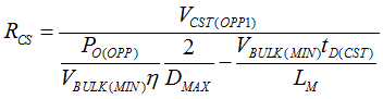
- where PO(OPP) is the output power that triggers OPP
- tD(CST) is the sum of all delays in the peak current loop which contributes additional peak current overshoot
tD(CST) consists of propagation delay of the low-side driver, current sense filter delay (ROPP x CCS), internal CS comparator delay (tD(CS)), and nonlinear capacitance delay of QL. After RCS is determined, ROPP can be adjusted to keep a similar OPP point at highest line. Note that setting the OPP trigger point too far away from the full power may introduce more challenge on the thermal design, since the converter runs continuously with more power as long as the corresponding peak current is slightly less than OPP threshold.
 Figure 8-43 VCST OPP curve across IVSL
 Figure 8-44 Timing Diagram of OPP