ZHCS614G October 2011 – September 2022 TPS40422
PRODUCTION DATA
- 1 特性
- 2 应用
- 3 说明
- 4 Revision History
- 5 说明(续)
- 6 Pin Configuration and Functions
- 7 Specifications
-
8 Detailed Description
- 8.1 Overview
- 8.2 Functional Block Diagram
- 8.3
Feature Description
- 8.3.1 PMBus Interface Protocol General Description
- 8.3.2 Voltage Reference
- 8.3.3 Output Voltage
- 8.3.4 Voltage Feed Forward
- 8.3.5 Current Sensing
- 8.3.6 Overcurrent Protection
- 8.3.7 Current Sharing
- 8.3.8 Linear Regulators
- 8.3.9 BP Switch-over
- 8.3.10 Switching Frequency Setting
- 8.3.11 Switching Node and BOOT Voltage
- 8.3.12 Reading the Output Current
- 8.3.13 Soft-Start Time
- 8.3.14 Turn-On/Turn-Off Delay and Sequencing
- 8.3.15 Pre-Biased Output Start-Up
- 8.3.16 Undervoltage Lockout
- 8.3.17 Overvoltage and Undervoltage Fault Protection
- 8.3.18 Power Good
- 8.3.19 Overtemperature Fault Protection
- 8.3.20 Thermal Shutdown
- 8.3.21 Programmable Fault Responses
- 8.3.22 User Data
- 8.3.23 Adjustable Anti-Cross Conduction Delay
- 8.3.24 Connection of Unused Pins
- 8.4 Device Functional Modes
- 8.5 Programming
- 8.6
Register Maps
- 8.6.1
Supported Commands
- 8.6.1.1 PAGE (00h)
- 8.6.1.2 OPERATION (01h)
- 8.6.1.3 ON_OFF_CONFIG (02h)
- 8.6.1.4 CLEAR_FAULTS (03h)
- 8.6.1.5 WRITE_PROTECT (10h)
- 8.6.1.6 STORE_USER_ALL (15h)
- 8.6.1.7 RESTORE_USER_ALL (16h)
- 8.6.1.8 CAPABILITY (19h)
- 8.6.1.9 VOUT_MODE (20h)
- 8.6.1.10 VIN_ON (35h)
- 8.6.1.11 VIN_OFF (36h)
- 8.6.1.12 IOUT_CAL_GAIN (38h)
- 8.6.1.13 IOUT_CAL_OFFSET (39h)
- 8.6.1.14 IOUT_OC_FAULT_LIMIT (46h)
- 8.6.1.15 IOUT_OC_FAULT_RESPONSE (47h)
- 8.6.1.16 IOUT_OC_WARN_LIMIT (4Ah)
- 8.6.1.17 OT_FAULT_LIMIT (4Fh)
- 8.6.1.18 OT_WARN_LIMIT (51h)
- 8.6.1.19 TON_RISE (61h)
- 8.6.1.20 STATUS_BYTE (78h)
- 8.6.1.21 STATUS_WORD (79h)
- 8.6.1.22 STATUS_VOUT (7Ah)
- 8.6.1.23 STATUS_IOUT (7Bh)
- 8.6.1.24 STATUS_TEMPERATURE (7Dh)
- 8.6.1.25 STATUS_CML (7Eh)
- 8.6.1.26 STATUS_MFR_SPECIFIC (80h)
- 8.6.1.27 READ_VOUT (8Bh)
- 8.6.1.28 READ_IOUT (8Ch)
- 8.6.1.29 READ_TEMPERATURE_2 (8Eh)
- 8.6.1.30 PMBUS_REVISION (98h)
- 8.6.1.31 MFR_SPECIFIC_00 (D0h)
- 8.6.1.32 VREF_TRIM (MFR_SPECIFIC_04) (D4h)
- 8.6.1.33 STEP_VREF_MARGIN_HIGH (MFR_SPECIFIC_05) (D5h)
- 8.6.1.34 STEP_VREF_MARGIN_LOW (MFR_SPECIFIC_06) (D6h)
- 8.6.1.35 PCT_VOUT_FAULT_PG_LIMIT (MFR_SPECIFIC_07) (D7h)
- 8.6.1.36 126
- 8.6.1.37 SEQUENCE_TON_TOFF_DELAY (MFR_SPECIFIC_08) (D8h)
- 8.6.1.38 128
- 8.6.1.39 OPTIONS (MFR_SPECIFIC_21) (E5h)
- 8.6.1.40 DEVICE_CODE (MFR_SPECIFIC_44) (FCh)
- 8.6.1
Supported Commands
-
9 Application and Implementation
- 9.1 Application Information
- 9.2
Typical Application
- 9.2.1
Dual-Output Converter
- 9.2.1.1 Design Requirements
- 9.2.1.2
Detailed Design Procedure
- 9.2.1.2.1 Custom Design with WEBENCH® Tools
- 9.2.1.2.2 Step 1: Inductor Selection
- 9.2.1.2.3 Step 2: Output Capacitor Selection
- 9.2.1.2.4 Step 3: Input Capacitance Selection
- 9.2.1.2.5 Step 4: MOSFET Selection
- 9.2.1.2.6 Step 5: Snubber Circuit Design
- 9.2.1.2.7 Step 6: Soft-Start Time
- 9.2.1.2.8
Step 7: Peripheral Component Design
- 9.2.1.2.8.1 RT (Pin 1) Switching Frequency Setting
- 9.2.1.2.8.2 FB1 (Pin 2) and FB2 (Pin 8) Output Voltage Setting
- 9.2.1.2.8.3 Compensation Network Using COMP1 (Pin 3) , COMP2 (Pin 7), FB1 (Pin 2) FB2 DIFFO1 (Pin 8) (Pin 39)
- 9.2.1.2.8.4 Remote Sensing Using VSNS1 (Pin 37), GSNS1 (Pin 38) , VSNS2 (Pin 15), and GSNS2 (Pin 14)
- 9.2.1.2.8.5 Temperate Sensing Using TSNS1 (Pin36) and TSNS2 (Pin 16)
- 9.2.1.2.8.6 Current Sensing Network Design Using CS1P (Pin 34), CS1N (Pin 35) , CS2P (Pin 18), and CS2N (Pin 17)
- 9.2.1.2.8.7 PMBus Address ADDR1 (Pin 9) , and ADDR0 (Pin 10)
- 9.2.1.2.8.8
Voltage Decoupling Capacitors
- 9.2.1.2.8.8.1 VDD (Pin 31)
- 9.2.1.2.8.8.2 BP3 (Pin 32)
- 9.2.1.2.8.8.3 BNEXT (Pin 24)
- 9.2.1.2.8.8.4 BP6 (Pin 25)
- 9.2.1.2.8.8.5 Power Good PGOOD1 (Pin 33), PGOOD2 (Pin 19)
- 9.2.1.2.8.8.6 Bootstrap Capacitors BOOT1 (Pin 30), and BOOT2 (Pin 20)
- 9.2.1.2.8.8.7 High-Side MOSFET (Gate) Resistor
- 9.2.1.2.8.8.8 Synchronization Setting SYNC (Pin 40)
- 9.2.1.2.8.8.9 BP6 (Pin 25)
- 9.2.1.2.8.8.10 DIFFO (Pin 39)
- 9.2.1.3 Application Curves
- 9.2.1
Dual-Output Converter
- 10Power Supply Recommendations
- 11Layout
- 12Device and Documentation Support
- 13Mechanical, Packaging, and Orderable Information
8.5.1.4 PMBus Interface Output Voltage Adjustment
The nominal output voltage of the converter can be adjusted using the VREF_TRIM command. See the VREF_TRIM command description for the format of this command as used in the TPS4022 device . The adjustment range is between -20% and +10% from the nominal output voltage. The VREF_TRIM command is typically used to trim the final output voltage of the converter without relying on high precision resistors being used in Figure 8-1. The resolution of the adjustment is 2 mV. The combination of margining and VREF_TRIM is limited to the range between –30% and +10% from the nominal output voltage. Exceeding this range is not supported.
The TPS4022 device operates in three states that determine the actual output voltage:
- No output margin
- Margin high
- Margin low
These output states are set using the OPERATION command. The FB pin reference voltage is calculated as follows in each of these states.
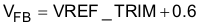
No margin voltage:
Margin high voltage state:

Margin low state:

where
- VFB is the FB pin voltage
- VREF_TRIM is the offset voltage in volts to be applied to the output voltage
- VREF_MARGIN_HIGH is the requested margin high voltage
- VREF_MARGIN_LOW is the requested margin low voltage