ZHCS614G October 2011 – September 2022 TPS40422
PRODUCTION DATA
- 1 特性
- 2 应用
- 3 说明
- 4 Revision History
- 5 说明(续)
- 6 Pin Configuration and Functions
- 7 Specifications
-
8 Detailed Description
- 8.1 Overview
- 8.2 Functional Block Diagram
- 8.3
Feature Description
- 8.3.1 PMBus Interface Protocol General Description
- 8.3.2 Voltage Reference
- 8.3.3 Output Voltage
- 8.3.4 Voltage Feed Forward
- 8.3.5 Current Sensing
- 8.3.6 Overcurrent Protection
- 8.3.7 Current Sharing
- 8.3.8 Linear Regulators
- 8.3.9 BP Switch-over
- 8.3.10 Switching Frequency Setting
- 8.3.11 Switching Node and BOOT Voltage
- 8.3.12 Reading the Output Current
- 8.3.13 Soft-Start Time
- 8.3.14 Turn-On/Turn-Off Delay and Sequencing
- 8.3.15 Pre-Biased Output Start-Up
- 8.3.16 Undervoltage Lockout
- 8.3.17 Overvoltage and Undervoltage Fault Protection
- 8.3.18 Power Good
- 8.3.19 Overtemperature Fault Protection
- 8.3.20 Thermal Shutdown
- 8.3.21 Programmable Fault Responses
- 8.3.22 User Data
- 8.3.23 Adjustable Anti-Cross Conduction Delay
- 8.3.24 Connection of Unused Pins
- 8.4 Device Functional Modes
- 8.5 Programming
- 8.6
Register Maps
- 8.6.1
Supported Commands
- 8.6.1.1 PAGE (00h)
- 8.6.1.2 OPERATION (01h)
- 8.6.1.3 ON_OFF_CONFIG (02h)
- 8.6.1.4 CLEAR_FAULTS (03h)
- 8.6.1.5 WRITE_PROTECT (10h)
- 8.6.1.6 STORE_USER_ALL (15h)
- 8.6.1.7 RESTORE_USER_ALL (16h)
- 8.6.1.8 CAPABILITY (19h)
- 8.6.1.9 VOUT_MODE (20h)
- 8.6.1.10 VIN_ON (35h)
- 8.6.1.11 VIN_OFF (36h)
- 8.6.1.12 IOUT_CAL_GAIN (38h)
- 8.6.1.13 IOUT_CAL_OFFSET (39h)
- 8.6.1.14 IOUT_OC_FAULT_LIMIT (46h)
- 8.6.1.15 IOUT_OC_FAULT_RESPONSE (47h)
- 8.6.1.16 IOUT_OC_WARN_LIMIT (4Ah)
- 8.6.1.17 OT_FAULT_LIMIT (4Fh)
- 8.6.1.18 OT_WARN_LIMIT (51h)
- 8.6.1.19 TON_RISE (61h)
- 8.6.1.20 STATUS_BYTE (78h)
- 8.6.1.21 STATUS_WORD (79h)
- 8.6.1.22 STATUS_VOUT (7Ah)
- 8.6.1.23 STATUS_IOUT (7Bh)
- 8.6.1.24 STATUS_TEMPERATURE (7Dh)
- 8.6.1.25 STATUS_CML (7Eh)
- 8.6.1.26 STATUS_MFR_SPECIFIC (80h)
- 8.6.1.27 READ_VOUT (8Bh)
- 8.6.1.28 READ_IOUT (8Ch)
- 8.6.1.29 READ_TEMPERATURE_2 (8Eh)
- 8.6.1.30 PMBUS_REVISION (98h)
- 8.6.1.31 MFR_SPECIFIC_00 (D0h)
- 8.6.1.32 VREF_TRIM (MFR_SPECIFIC_04) (D4h)
- 8.6.1.33 STEP_VREF_MARGIN_HIGH (MFR_SPECIFIC_05) (D5h)
- 8.6.1.34 STEP_VREF_MARGIN_LOW (MFR_SPECIFIC_06) (D6h)
- 8.6.1.35 PCT_VOUT_FAULT_PG_LIMIT (MFR_SPECIFIC_07) (D7h)
- 8.6.1.36 126
- 8.6.1.37 SEQUENCE_TON_TOFF_DELAY (MFR_SPECIFIC_08) (D8h)
- 8.6.1.38 128
- 8.6.1.39 OPTIONS (MFR_SPECIFIC_21) (E5h)
- 8.6.1.40 DEVICE_CODE (MFR_SPECIFIC_44) (FCh)
- 8.6.1
Supported Commands
-
9 Application and Implementation
- 9.1 Application Information
- 9.2
Typical Application
- 9.2.1
Dual-Output Converter
- 9.2.1.1 Design Requirements
- 9.2.1.2
Detailed Design Procedure
- 9.2.1.2.1 Custom Design with WEBENCH® Tools
- 9.2.1.2.2 Step 1: Inductor Selection
- 9.2.1.2.3 Step 2: Output Capacitor Selection
- 9.2.1.2.4 Step 3: Input Capacitance Selection
- 9.2.1.2.5 Step 4: MOSFET Selection
- 9.2.1.2.6 Step 5: Snubber Circuit Design
- 9.2.1.2.7 Step 6: Soft-Start Time
- 9.2.1.2.8
Step 7: Peripheral Component Design
- 9.2.1.2.8.1 RT (Pin 1) Switching Frequency Setting
- 9.2.1.2.8.2 FB1 (Pin 2) and FB2 (Pin 8) Output Voltage Setting
- 9.2.1.2.8.3 Compensation Network Using COMP1 (Pin 3) , COMP2 (Pin 7), FB1 (Pin 2) FB2 DIFFO1 (Pin 8) (Pin 39)
- 9.2.1.2.8.4 Remote Sensing Using VSNS1 (Pin 37), GSNS1 (Pin 38) , VSNS2 (Pin 15), and GSNS2 (Pin 14)
- 9.2.1.2.8.5 Temperate Sensing Using TSNS1 (Pin36) and TSNS2 (Pin 16)
- 9.2.1.2.8.6 Current Sensing Network Design Using CS1P (Pin 34), CS1N (Pin 35) , CS2P (Pin 18), and CS2N (Pin 17)
- 9.2.1.2.8.7 PMBus Address ADDR1 (Pin 9) , and ADDR0 (Pin 10)
- 9.2.1.2.8.8
Voltage Decoupling Capacitors
- 9.2.1.2.8.8.1 VDD (Pin 31)
- 9.2.1.2.8.8.2 BP3 (Pin 32)
- 9.2.1.2.8.8.3 BNEXT (Pin 24)
- 9.2.1.2.8.8.4 BP6 (Pin 25)
- 9.2.1.2.8.8.5 Power Good PGOOD1 (Pin 33), PGOOD2 (Pin 19)
- 9.2.1.2.8.8.6 Bootstrap Capacitors BOOT1 (Pin 30), and BOOT2 (Pin 20)
- 9.2.1.2.8.8.7 High-Side MOSFET (Gate) Resistor
- 9.2.1.2.8.8.8 Synchronization Setting SYNC (Pin 40)
- 9.2.1.2.8.8.9 BP6 (Pin 25)
- 9.2.1.2.8.8.10 DIFFO (Pin 39)
- 9.2.1.3 Application Curves
- 9.2.1
Dual-Output Converter
- 10Power Supply Recommendations
- 11Layout
- 12Device and Documentation Support
- 13Mechanical, Packaging, and Orderable Information
8.3.5 Current Sensing
The TPS4022 device uses a differential current-sense scheme to sense the output current. The sense element can be either the series resistance of the power stage filter inductor or a separate current sense resistor. When using the inductor series resistance as in Figure 8-2, a filter must be used to remove the large AC component of voltage across the inductor and leave only the component of the voltage that appears across the resistance of the inductor. The values of R5 and C4 for the ideal case can be found using Equation 2. The time constant of the R-C filter should be equal to or greater than the time constant of the inductor itself. If the time constants are equal, the voltage appearing across C4 is the current in the inductor multiplied the inductor resistance. The voltage across C4 perfectly reflects the inductor ripple current. Therefore, there is no need to have a shorter R-C time constant.
Extending the R-C filter time constant beyond the inductor time constant lowers the AC ripple component of voltage present at the current sense pins of the device, but allows the correct DC current information to remain intact. This extension also delays slightly the response to an overcurrent event, but reduces noise in the system leading to cleaner overcurrent performance and current reporting data over the PMBus interface.
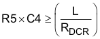
where (from Figure 8-2)
- R5 and RESR are in Ω
- C4 is in F (suggest 100 nF, 10-7F)
- L is in H
TPS4022 device is designed to accept a maximum voltage of 60 mV across the current-sense pins. Most inductors have a copper conductor which results in a fairly large temperature coefficient of resistance. Because of this large temperature coefficient, the resistance of the inductor and the current through the inductor should make a peak voltage less than 60 mV when the inductor is at the maximum temperature for the converter. This situation also applies for the external resistor in Figure 8-3. The full-load output current multiplied by the sense resistor value, must be less than 60 mV at the maximum converter operating temperature.
In all cases, C4 should be placed as close to the current sense pins as possible to help avoid problems with noise.
 Figure 8-2 Current Sensing Using Inductor Resistance
 Figure 8-3 Current Sensing Using Sense Resistor
After choosing the current sensing method, set the current-sense element resistance. This value allows the proper calculation of thresholds for the overcurrent fault and warning, as well as more accurate reporting of the actual output current. The IOUT_CAL_GAIN command is used to set the value of the sense element resistance of the device. IOUT_OC_WARN_LIMIT and IOUT_OC_FAULT_LIMIT set the levels for the overcurrent warning and fault levels respectively. (See the Section 8.5.1 section for more details.)