ZHCS614G October 2011 – September 2022 TPS40422
PRODUCTION DATA
- 1 特性
- 2 应用
- 3 说明
- 4 Revision History
- 5 说明(续)
- 6 Pin Configuration and Functions
- 7 Specifications
-
8 Detailed Description
- 8.1 Overview
- 8.2 Functional Block Diagram
- 8.3
Feature Description
- 8.3.1 PMBus Interface Protocol General Description
- 8.3.2 Voltage Reference
- 8.3.3 Output Voltage
- 8.3.4 Voltage Feed Forward
- 8.3.5 Current Sensing
- 8.3.6 Overcurrent Protection
- 8.3.7 Current Sharing
- 8.3.8 Linear Regulators
- 8.3.9 BP Switch-over
- 8.3.10 Switching Frequency Setting
- 8.3.11 Switching Node and BOOT Voltage
- 8.3.12 Reading the Output Current
- 8.3.13 Soft-Start Time
- 8.3.14 Turn-On/Turn-Off Delay and Sequencing
- 8.3.15 Pre-Biased Output Start-Up
- 8.3.16 Undervoltage Lockout
- 8.3.17 Overvoltage and Undervoltage Fault Protection
- 8.3.18 Power Good
- 8.3.19 Overtemperature Fault Protection
- 8.3.20 Thermal Shutdown
- 8.3.21 Programmable Fault Responses
- 8.3.22 User Data
- 8.3.23 Adjustable Anti-Cross Conduction Delay
- 8.3.24 Connection of Unused Pins
- 8.4 Device Functional Modes
- 8.5 Programming
- 8.6
Register Maps
- 8.6.1
Supported Commands
- 8.6.1.1 PAGE (00h)
- 8.6.1.2 OPERATION (01h)
- 8.6.1.3 ON_OFF_CONFIG (02h)
- 8.6.1.4 CLEAR_FAULTS (03h)
- 8.6.1.5 WRITE_PROTECT (10h)
- 8.6.1.6 STORE_USER_ALL (15h)
- 8.6.1.7 RESTORE_USER_ALL (16h)
- 8.6.1.8 CAPABILITY (19h)
- 8.6.1.9 VOUT_MODE (20h)
- 8.6.1.10 VIN_ON (35h)
- 8.6.1.11 VIN_OFF (36h)
- 8.6.1.12 IOUT_CAL_GAIN (38h)
- 8.6.1.13 IOUT_CAL_OFFSET (39h)
- 8.6.1.14 IOUT_OC_FAULT_LIMIT (46h)
- 8.6.1.15 IOUT_OC_FAULT_RESPONSE (47h)
- 8.6.1.16 IOUT_OC_WARN_LIMIT (4Ah)
- 8.6.1.17 OT_FAULT_LIMIT (4Fh)
- 8.6.1.18 OT_WARN_LIMIT (51h)
- 8.6.1.19 TON_RISE (61h)
- 8.6.1.20 STATUS_BYTE (78h)
- 8.6.1.21 STATUS_WORD (79h)
- 8.6.1.22 STATUS_VOUT (7Ah)
- 8.6.1.23 STATUS_IOUT (7Bh)
- 8.6.1.24 STATUS_TEMPERATURE (7Dh)
- 8.6.1.25 STATUS_CML (7Eh)
- 8.6.1.26 STATUS_MFR_SPECIFIC (80h)
- 8.6.1.27 READ_VOUT (8Bh)
- 8.6.1.28 READ_IOUT (8Ch)
- 8.6.1.29 READ_TEMPERATURE_2 (8Eh)
- 8.6.1.30 PMBUS_REVISION (98h)
- 8.6.1.31 MFR_SPECIFIC_00 (D0h)
- 8.6.1.32 VREF_TRIM (MFR_SPECIFIC_04) (D4h)
- 8.6.1.33 STEP_VREF_MARGIN_HIGH (MFR_SPECIFIC_05) (D5h)
- 8.6.1.34 STEP_VREF_MARGIN_LOW (MFR_SPECIFIC_06) (D6h)
- 8.6.1.35 PCT_VOUT_FAULT_PG_LIMIT (MFR_SPECIFIC_07) (D7h)
- 8.6.1.36 126
- 8.6.1.37 SEQUENCE_TON_TOFF_DELAY (MFR_SPECIFIC_08) (D8h)
- 8.6.1.38 128
- 8.6.1.39 OPTIONS (MFR_SPECIFIC_21) (E5h)
- 8.6.1.40 DEVICE_CODE (MFR_SPECIFIC_44) (FCh)
- 8.6.1
Supported Commands
-
9 Application and Implementation
- 9.1 Application Information
- 9.2
Typical Application
- 9.2.1
Dual-Output Converter
- 9.2.1.1 Design Requirements
- 9.2.1.2
Detailed Design Procedure
- 9.2.1.2.1 Custom Design with WEBENCH® Tools
- 9.2.1.2.2 Step 1: Inductor Selection
- 9.2.1.2.3 Step 2: Output Capacitor Selection
- 9.2.1.2.4 Step 3: Input Capacitance Selection
- 9.2.1.2.5 Step 4: MOSFET Selection
- 9.2.1.2.6 Step 5: Snubber Circuit Design
- 9.2.1.2.7 Step 6: Soft-Start Time
- 9.2.1.2.8
Step 7: Peripheral Component Design
- 9.2.1.2.8.1 RT (Pin 1) Switching Frequency Setting
- 9.2.1.2.8.2 FB1 (Pin 2) and FB2 (Pin 8) Output Voltage Setting
- 9.2.1.2.8.3 Compensation Network Using COMP1 (Pin 3) , COMP2 (Pin 7), FB1 (Pin 2) FB2 DIFFO1 (Pin 8) (Pin 39)
- 9.2.1.2.8.4 Remote Sensing Using VSNS1 (Pin 37), GSNS1 (Pin 38) , VSNS2 (Pin 15), and GSNS2 (Pin 14)
- 9.2.1.2.8.5 Temperate Sensing Using TSNS1 (Pin36) and TSNS2 (Pin 16)
- 9.2.1.2.8.6 Current Sensing Network Design Using CS1P (Pin 34), CS1N (Pin 35) , CS2P (Pin 18), and CS2N (Pin 17)
- 9.2.1.2.8.7 PMBus Address ADDR1 (Pin 9) , and ADDR0 (Pin 10)
- 9.2.1.2.8.8
Voltage Decoupling Capacitors
- 9.2.1.2.8.8.1 VDD (Pin 31)
- 9.2.1.2.8.8.2 BP3 (Pin 32)
- 9.2.1.2.8.8.3 BNEXT (Pin 24)
- 9.2.1.2.8.8.4 BP6 (Pin 25)
- 9.2.1.2.8.8.5 Power Good PGOOD1 (Pin 33), PGOOD2 (Pin 19)
- 9.2.1.2.8.8.6 Bootstrap Capacitors BOOT1 (Pin 30), and BOOT2 (Pin 20)
- 9.2.1.2.8.8.7 High-Side MOSFET (Gate) Resistor
- 9.2.1.2.8.8.8 Synchronization Setting SYNC (Pin 40)
- 9.2.1.2.8.8.9 BP6 (Pin 25)
- 9.2.1.2.8.8.10 DIFFO (Pin 39)
- 9.2.1.3 Application Curves
- 9.2.1
Dual-Output Converter
- 10Power Supply Recommendations
- 11Layout
- 12Device and Documentation Support
- 13Mechanical, Packaging, and Orderable Information
8.3.3 Output Voltage
The TPS4022 device sets the output voltage in a way that is very similar to a traditional analog controller by using a voltage divider from the output to the FB (feedback) pin. The output voltage must be divided down to the nominal reference voltage of 600 mV. Figure 8-1 shows the typical connections for the controller. The device senses the voltage at the load by using the unity gain differential voltage sense amplifier. This functionality provides better load regulation for output voltages lower than 5-V nominal (see the Section 7.5 table for the maximum output voltage specification for the differential sense amplifier). For output voltages above this level, connect the output voltage directly to the junction of R1 and C1, leave DIFFO1 open, and do not connect the VSNS1 pin to the output voltage. The differential amplifier may also be used elsewhere in the overall system as a voltage buffer, provided the electrical specifications are not exceeded.
 Figure 8-1 Setting the Output Voltage
The components shown in Figure 8-1 that determine the nominal output voltage are R1 and R2. In most cases, choose a value for R to ensure the feedback compensation values (R3, R4, C1, C2 and C3) come close to readily available standard values. A value for R2 is then calculated in Equation 1.
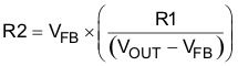
where
- VFB is the feedback voltage
- VOUT is the desired output voltage
- R1 and R2 are in the same unit
There is no DIFFO2 pin. In dual-output mode, VSNS2 and GSNS2 are connected to the load for channel 2 and the device uses the DIFFO2 signal internally to provide voltage monitoring. Connect the output directly to the junction of R1 and C1 for channel 2 to set the output voltage and for feedback.
The DIFFO1 pin operates at voltages up to (VBP6–0.2 V). If the voltage between the VSNS1 and GSNS1 pins is higher than (VBP6–0.2 V) during any condition, the output voltage moves out of regulation because the DIFFO1 voltage is limited by BP6. To prevent this from happening, the BP6 voltage must be pre-biased before the PWM turns on, and (VBP6–0.2 V) must remain higher than the voltage between the VSNS1 and GSNS1 pins until the PWM turns off.
The feedback voltage can be changed to a value between –30% and +10% from the nominal 600 mV using PMBus commands. This adjustment allows the output voltage to vary by the same percentage. See the Section 8.5.1 section for more details.