ZHCS614G October 2011 – September 2022 TPS40422
PRODUCTION DATA
- 1 特性
- 2 应用
- 3 说明
- 4 Revision History
- 5 说明(续)
- 6 Pin Configuration and Functions
- 7 Specifications
-
8 Detailed Description
- 8.1 Overview
- 8.2 Functional Block Diagram
- 8.3
Feature Description
- 8.3.1 PMBus Interface Protocol General Description
- 8.3.2 Voltage Reference
- 8.3.3 Output Voltage
- 8.3.4 Voltage Feed Forward
- 8.3.5 Current Sensing
- 8.3.6 Overcurrent Protection
- 8.3.7 Current Sharing
- 8.3.8 Linear Regulators
- 8.3.9 BP Switch-over
- 8.3.10 Switching Frequency Setting
- 8.3.11 Switching Node and BOOT Voltage
- 8.3.12 Reading the Output Current
- 8.3.13 Soft-Start Time
- 8.3.14 Turn-On/Turn-Off Delay and Sequencing
- 8.3.15 Pre-Biased Output Start-Up
- 8.3.16 Undervoltage Lockout
- 8.3.17 Overvoltage and Undervoltage Fault Protection
- 8.3.18 Power Good
- 8.3.19 Overtemperature Fault Protection
- 8.3.20 Thermal Shutdown
- 8.3.21 Programmable Fault Responses
- 8.3.22 User Data
- 8.3.23 Adjustable Anti-Cross Conduction Delay
- 8.3.24 Connection of Unused Pins
- 8.4 Device Functional Modes
- 8.5 Programming
- 8.6
Register Maps
- 8.6.1
Supported Commands
- 8.6.1.1 PAGE (00h)
- 8.6.1.2 OPERATION (01h)
- 8.6.1.3 ON_OFF_CONFIG (02h)
- 8.6.1.4 CLEAR_FAULTS (03h)
- 8.6.1.5 WRITE_PROTECT (10h)
- 8.6.1.6 STORE_USER_ALL (15h)
- 8.6.1.7 RESTORE_USER_ALL (16h)
- 8.6.1.8 CAPABILITY (19h)
- 8.6.1.9 VOUT_MODE (20h)
- 8.6.1.10 VIN_ON (35h)
- 8.6.1.11 VIN_OFF (36h)
- 8.6.1.12 IOUT_CAL_GAIN (38h)
- 8.6.1.13 IOUT_CAL_OFFSET (39h)
- 8.6.1.14 IOUT_OC_FAULT_LIMIT (46h)
- 8.6.1.15 IOUT_OC_FAULT_RESPONSE (47h)
- 8.6.1.16 IOUT_OC_WARN_LIMIT (4Ah)
- 8.6.1.17 OT_FAULT_LIMIT (4Fh)
- 8.6.1.18 OT_WARN_LIMIT (51h)
- 8.6.1.19 TON_RISE (61h)
- 8.6.1.20 STATUS_BYTE (78h)
- 8.6.1.21 STATUS_WORD (79h)
- 8.6.1.22 STATUS_VOUT (7Ah)
- 8.6.1.23 STATUS_IOUT (7Bh)
- 8.6.1.24 STATUS_TEMPERATURE (7Dh)
- 8.6.1.25 STATUS_CML (7Eh)
- 8.6.1.26 STATUS_MFR_SPECIFIC (80h)
- 8.6.1.27 READ_VOUT (8Bh)
- 8.6.1.28 READ_IOUT (8Ch)
- 8.6.1.29 READ_TEMPERATURE_2 (8Eh)
- 8.6.1.30 PMBUS_REVISION (98h)
- 8.6.1.31 MFR_SPECIFIC_00 (D0h)
- 8.6.1.32 VREF_TRIM (MFR_SPECIFIC_04) (D4h)
- 8.6.1.33 STEP_VREF_MARGIN_HIGH (MFR_SPECIFIC_05) (D5h)
- 8.6.1.34 STEP_VREF_MARGIN_LOW (MFR_SPECIFIC_06) (D6h)
- 8.6.1.35 PCT_VOUT_FAULT_PG_LIMIT (MFR_SPECIFIC_07) (D7h)
- 8.6.1.36 126
- 8.6.1.37 SEQUENCE_TON_TOFF_DELAY (MFR_SPECIFIC_08) (D8h)
- 8.6.1.38 128
- 8.6.1.39 OPTIONS (MFR_SPECIFIC_21) (E5h)
- 8.6.1.40 DEVICE_CODE (MFR_SPECIFIC_44) (FCh)
- 8.6.1
Supported Commands
-
9 Application and Implementation
- 9.1 Application Information
- 9.2
Typical Application
- 9.2.1
Dual-Output Converter
- 9.2.1.1 Design Requirements
- 9.2.1.2
Detailed Design Procedure
- 9.2.1.2.1 Custom Design with WEBENCH® Tools
- 9.2.1.2.2 Step 1: Inductor Selection
- 9.2.1.2.3 Step 2: Output Capacitor Selection
- 9.2.1.2.4 Step 3: Input Capacitance Selection
- 9.2.1.2.5 Step 4: MOSFET Selection
- 9.2.1.2.6 Step 5: Snubber Circuit Design
- 9.2.1.2.7 Step 6: Soft-Start Time
- 9.2.1.2.8
Step 7: Peripheral Component Design
- 9.2.1.2.8.1 RT (Pin 1) Switching Frequency Setting
- 9.2.1.2.8.2 FB1 (Pin 2) and FB2 (Pin 8) Output Voltage Setting
- 9.2.1.2.8.3 Compensation Network Using COMP1 (Pin 3) , COMP2 (Pin 7), FB1 (Pin 2) FB2 DIFFO1 (Pin 8) (Pin 39)
- 9.2.1.2.8.4 Remote Sensing Using VSNS1 (Pin 37), GSNS1 (Pin 38) , VSNS2 (Pin 15), and GSNS2 (Pin 14)
- 9.2.1.2.8.5 Temperate Sensing Using TSNS1 (Pin36) and TSNS2 (Pin 16)
- 9.2.1.2.8.6 Current Sensing Network Design Using CS1P (Pin 34), CS1N (Pin 35) , CS2P (Pin 18), and CS2N (Pin 17)
- 9.2.1.2.8.7 PMBus Address ADDR1 (Pin 9) , and ADDR0 (Pin 10)
- 9.2.1.2.8.8
Voltage Decoupling Capacitors
- 9.2.1.2.8.8.1 VDD (Pin 31)
- 9.2.1.2.8.8.2 BP3 (Pin 32)
- 9.2.1.2.8.8.3 BNEXT (Pin 24)
- 9.2.1.2.8.8.4 BP6 (Pin 25)
- 9.2.1.2.8.8.5 Power Good PGOOD1 (Pin 33), PGOOD2 (Pin 19)
- 9.2.1.2.8.8.6 Bootstrap Capacitors BOOT1 (Pin 30), and BOOT2 (Pin 20)
- 9.2.1.2.8.8.7 High-Side MOSFET (Gate) Resistor
- 9.2.1.2.8.8.8 Synchronization Setting SYNC (Pin 40)
- 9.2.1.2.8.8.9 BP6 (Pin 25)
- 9.2.1.2.8.8.10 DIFFO (Pin 39)
- 9.2.1.3 Application Curves
- 9.2.1
Dual-Output Converter
- 10Power Supply Recommendations
- 11Layout
- 12Device and Documentation Support
- 13Mechanical, Packaging, and Orderable Information
9.2.1.2.3 Step 2: Output Capacitor Selection
The output capacitor is typically selected by the output load transient-response requirement and by allowable output voltage ripple.
- The output capacitor must supply the load with the required current when it is not immediately provided by the regulator. When the output capacitor supplies load current, the impedance of the capacitor affects the magnitude of voltage deviation during the transient.
- The ripple voltage developed across the output capacitor is due to the ripple current in the capacitor and in turn the ripple current is usually due to either the ESR or the value of the capacitor. The ESR of aluminum electrolytics and most tantalums are too high to allow for effective ripple reduction. Often, a combination of several electrolytic capacitors have to be paralleled to obtain large enough value of capacitance with low enough ESR in addition to several ceramic capacitors that offer much lower ESR but at the price of lower capacitance value.
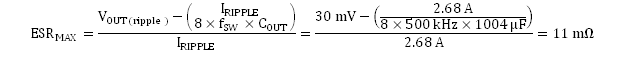
Equation 23 calculates the minimum output capacitance needed to satisfy overvoltage and undervoltage requirements during the load step. In practical design to account for de-rating and variation it is strongly recommended to multiply the calculated capacitance value by a factor between 1.5 and 5 based on the tests in the actual circuit. In this example, two 330-µF polymer capacitors with ESR of 15 mΩ were chosen as well as three 100-µF ceramic capacitor with ESR of 3 mΩ. The total equivalent capacitance COUT is 1004 µF. The additional 0.1-µF capacitor (C38 and C39) is used for filtering of high frequency noise.

where
- ITRAN(min) is the load transient step
- ∆VOUT is the output voltage deviation during load transient
- COUT(min) is the minimum required capacitance
Using the known target output capacitance value, Equation 24 calculates the maximum ESR allowed to meet the output voltage ripple specification.