ZHCSJC6F March 2016 – June 2018 TDA2E
PRODUCTION DATA.
- 1 器件概述
- 2 修订历史记录
- 3 Device Comparison
-
4 Terminal Configuration and Functions
- 4.1 Terminal Assignment
- 4.2 Ball Characteristics
- 4.3 Multiplexing Characteristics
- 4.4
Signal Descriptions
- 4.4.1 Video Input Ports (VIP)
- 4.4.2 Display Subsystem – Video Output Ports
- 4.4.3 Display Subsystem – High-Definition Multimedia Interface (HDMI)
- 4.4.4 Camera Serial Interface 2 CAL bridge (CSI2)
- 4.4.5 External Memory Interface (EMIF SDRAM)
- 4.4.6 General-Purpose Memory Controller (GPMC)
- 4.4.7 Timers
- 4.4.8 Inter-Integrated Circuit Interface (I2C)
- 4.4.9 Universal Asynchronous Receiver Transmitter (UART)
- 4.4.10 Multichannel Serial Peripheral Interface (McSPI)
- 4.4.11 Quad Serial Peripheral Interface (QSPI)
- 4.4.12 Multichannel Audio Serial Port (McASP)
- 4.4.13 Universal Serial Bus (USB)
- 4.4.14 SATA
- 4.4.15 Peripheral Component Interconnect Express (PCIe)
- 4.4.16 Controller Area Network Interface (DCAN)
- 4.4.17 Ethernet Interface (GMAC_SW)
- 4.4.18 eMMC/SD/SDIO
- 4.4.19 General-Purpose Interface (GPIO)
- 4.4.20 Pulse Width Modulation (PWM) Interface
- 4.4.21 Test Interfaces
- 4.4.22 System and Miscellaneous
- 4.4.23 Power Supplies
-
5 Specifications
- 5.1 Absolute Maximum Ratings
- 5.2 ESD Ratings
- 5.3 Power on Hour (POH) Limits
- 5.4 Recommended Operating Conditions
- 5.5 Operating Performance Points
- 5.6 Power Consumption Summary
- 5.7
Electrical Characteristics
- 5.7.1 LVCMOS DDR DC Electrical Characteristics
- 5.7.2 HDMIPHY DC Electrical Characteristics
- 5.7.3 Dual Voltage LVCMOS I2C DC Electrical Characteristics
- 5.7.4 IQ1833 Buffers DC Electrical Characteristics
- 5.7.5 IHHV1833 Buffers DC Electrical Characteristics
- 5.7.6 LVCMOS CSI2 DC Electrical Characteristics
- 5.7.7 BC1833IHHV Buffers DC Electrical Characteristics
- 5.7.8 USBPHY DC Electrical Characteristics
- 5.7.9 Dual Voltage SDIO1833 DC Electrical Characteristics
- 5.7.10 Dual Voltage LVCMOS DC Electrical Characteristics
- 5.7.11 SATAPHY DC Electrical Characteristics
- 5.7.12 PCIEPHY DC Electrical Characteristics
- 5.8 Thermal Characteristics
- 5.9 Power Supply Sequences
- 6 Clock Specifications
-
7 Timing Requirements and Switching Characteristics
- 7.1 Timing Test Conditions
- 7.2 Interface Clock Specifications
- 7.3 Timing Parameters and Information
- 7.4 Recommended Clock and Control Signal Transition Behavior
- 7.5 Virtual and Manual I/O Timing Modes
- 7.6 Video Input Ports (VIP)
- 7.7 Display Subsystem - Video Output Ports
- 7.8 Display Subsystem - High-Definition Multimedia Interface (HDMI)
- 7.9 Camera Serial Interface 2 CAL bridge (CSI2)
- 7.10 External Memory Interface (EMIF)
- 7.11 General-Purpose Memory Controller (GPMC)
- 7.12 Timers
- 7.13 Inter-Integrated Circuit Interface (I2C)
- 7.14 Universal Asynchronous Receiver Transmitter (UART)
- 7.15 Multichannel Serial Peripheral Interface (McSPI)
- 7.16 Quad Serial Peripheral Interface (QSPI)
- 7.17 Multichannel Audio Serial Port (McASP)
- 7.18 Universal Serial Bus (USB)
- 7.19 Serial Advanced Technology Attachment (SATA)
- 7.20 Peripheral Component Interconnect Express (PCIe)
- 7.21 Controller Area Network Interface (DCAN)
- 7.22
Ethernet Interface (GMAC_SW)
- 7.22.1
GMAC MII Timings
- Table 7-66 Timing Requirements for miin_rxclk - MII Operation
- Table 7-67 Timing Requirements for miin_txclk - MII Operation
- Table 7-68 Timing Requirements for GMAC MIIn Receive 10/100 Mbit/s
- Table 7-69 Switching Characteristics Over Recommended Operating Conditions for GMAC MIIn Transmit 10/100 Mbits/s
- 7.22.2 GMAC MDIO Interface Timings
- 7.22.3
GMAC RMII Timings
- Table 7-74 Timing Requirements for GMAC REF_CLK - RMII Operation
- Table 7-75 Timing Requirements for GMAC RMIIn Receive
- Table 7-76 Switching Characteristics Over Recommended Operating Conditions for GMAC REF_CLK - RMII Operation
- Table 7-77 Switching Characteristics Over Recommended Operating Conditions for GMAC RMIIn Transmit 10/100 Mbits/s
- 7.22.4
GMAC RGMII Timings
- Table 7-81 Timing Requirements for rgmiin_rxc - RGMIIn Operation
- Table 7-82 Timing Requirements for GMAC RGMIIn Input Receive for 10/100/1000 Mbps
- Table 7-83 Switching Characteristics Over Recommended Operating Conditions for rgmiin_txctl - RGMIIn Operation for 10/100/1000 Mbit/s
- Table 7-84 Switching Characteristics for GMAC RGMIIn Output Transmit for 10/100/1000 Mbps
- 7.22.1
GMAC MII Timings
- 7.23
eMMC/SD/SDIO
- 7.23.1
MMC1-SD Card Interface
- 7.23.1.1 Default speed, 4-bit data, SDR, half-cycle
- 7.23.1.2 High speed, 4-bit data, SDR, half-cycle
- 7.23.1.3 SDR12, 4-bit data, half-cycle
- 7.23.1.4 SDR25, 4-bit data, half-cycle
- 7.23.1.5 UHS-I SDR50, 4-bit data, half-cycle
- 7.23.1.6 UHS-I SDR104, 4-bit data, half-cycle
- 7.23.1.7 UHS-I DDR50, 4-bit data
- 7.23.2 MMC2 - eMMC
- 7.23.3 MMC3 and MMC4-SDIO/SD
- 7.23.1
MMC1-SD Card Interface
- 7.24 General-Purpose Interface (GPIO)
- 7.25 System and Miscellaneous interfaces
- 7.26
Test Interfaces
- 7.26.1
IEEE 1149.1 Standard-Test-Access Port (JTAG)
- 7.26.1.1
JTAG Electrical Data/Timing
- Table 7-131 Timing Requirements for IEEE 1149.1 JTAG
- Table 7-132 Switching Characteristics Over Recommended Operating Conditions for IEEE 1149.1 JTAG
- Table 7-133 Timing Requirements for IEEE 1149.1 JTAG With RTCK
- Table 7-134 Switching Characteristics Over Recommended Operating Conditions for IEEE 1149.1 JTAG With RTCK
- 7.26.1.1
JTAG Electrical Data/Timing
- 7.26.2 Trace Port Interface Unit (TPIU)
- 7.26.1
IEEE 1149.1 Standard-Test-Access Port (JTAG)
-
8 Applications, Implementation, and Layout
- 8.1 Introduction
- 8.2 Power Optimizations
- 8.3 Core Power Domains
- 8.4 Single-Ended Interfaces
- 8.5
Differential Interfaces
- 8.5.1 General Routing Guidelines
- 8.5.2
USB 2.0 Board Design and Layout Guidelines
- 8.5.2.1 Background
- 8.5.2.2
USB PHY Layout Guide
- 8.5.2.2.1 General Routing and Placement
- 8.5.2.2.2
Specific Guidelines for USB PHY Layout
- 8.5.2.2.2.1 Analog, PLL, and Digital Power Supply Filtering
- 8.5.2.2.2.2 Analog, Digital, and PLL Partitioning
- 8.5.2.2.2.3 Board Stackup
- 8.5.2.2.2.4 Cable Connector Socket
- 8.5.2.2.2.5 Clock Routings
- 8.5.2.2.2.6 Crystals/Oscillator
- 8.5.2.2.2.7 DP/DM Trace
- 8.5.2.2.2.8 DP/DM Vias
- 8.5.2.2.2.9 Image Planes
- 8.5.2.2.2.10 Power Regulators
- 8.5.2.3 References
- 8.5.3 USB 3.0 Board Design and Layout Guidelines
- 8.5.4 HDMI Board Design and Layout Guidelines
- 8.5.5 PCIe Board Design and Layout Guidelines
- 8.5.6 CSI2 Board Design and Routing Guidelines
- 8.6
DDR3 Board Design and Layout Guidelines
- 8.6.1 DDR3 General Board Layout Guidelines
- 8.6.2
DDR3 Board Design and Layout Guidelines
- 8.6.2.1 Board Designs
- 8.6.2.2 DDR3 EMIF
- 8.6.2.3 DDR3 Device Combinations
- 8.6.2.4 DDR3 Interface Schematic
- 8.6.2.5 Compatible JEDEC DDR3 Devices
- 8.6.2.6 PCB Stackup
- 8.6.2.7 Placement
- 8.6.2.8 DDR3 Keepout Region
- 8.6.2.9 Bulk Bypass Capacitors
- 8.6.2.10 High-Speed Bypass Capacitors
- 8.6.2.11 Net Classes
- 8.6.2.12 DDR3 Signal Termination
- 8.6.2.13 VREF_DDR Routing
- 8.6.2.14 VTT
- 8.6.2.15 CK and ADDR_CTRL Topologies and Routing Definition
- 8.6.2.16 Data Topologies and Routing Definition
- 8.6.2.17 Routing Specification
- 9 Device and Documentation Support
- 10Mechanical Packaging Information
5.9 Power Supply Sequences
This section describes the power-up and power-down sequence required to ensure proper device operation. The power supply names described in this section comprise a superset of a family of compatible devices. Some members of this family will not include a subset of these power supplies and their associated device modules. Refer to the Section 4.2, Ball Characteristics of the Section 4, Terminal Configuration and Functions to determine which power supplies are applicable.
Figure 5-2 and Figure 5-3 describe the device Power Sequencing when RTC-mode is used.
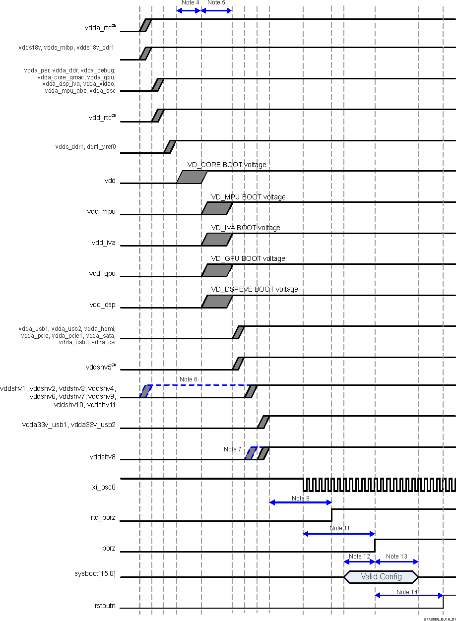 Figure 5-2 Power-Up Sequencing
 - Grey shaded areas are windows where it is valid to ramp the voltage rail.
- Blue dashed lines are not valid windows but show alternate ramp possibilities based on the associated note.
- If RTC-mode is used then vdda_rtc, vdd_rtc and vddshv5 must be individually powered with separate power supplies and cannot be combined with other rails.
- vdd must ramp before or at the same time as vdd_mpu, vdd_gpu, vdd_dsp and vdd_iva.
- vdd_mpu, vdd_gpu, vdd_dsp, vdd_iva can be ramped at the same time or can be staggered.
- If any of the vddshv[1-7,9-11] rails (not including vddshv8) are used as 1.8V only, then these rails can be combined with vdds18v.
- vddshv8 is separated out to show support for dual voltage. If single voltage is used then vddshv8 can be combined with other vddshvn rails but vddshv8 must ramp after vdd.
- vdds and vdda rails must not be combined together.
- Pulse duration: rtc_porz must remain low 1ms after vdda_rtc, vddshv5, and vdd_rtc are ramped and stable.
- The SYS_32K source must be stable and at a valid frequency 1ms prior to de-asserting rtc_porz high.
- Pulse duration: porz must remain low a minimum of 12P(15) after xi_osc0 is stable and at a valid frequency. porz must also remain low until all supply rails are valid and stable. resetn must be high prior to, or simultaneous with, porz rising. During initial power-up, resetn can rise any time after, or concurrently with, its supply voltage, vddshv3 rising.
- Setup time: sysboot[15:0] pins must be valid 2P(15) before porz is de-asserted high.
- Hold time: sysboot[15:0] pins must be valid 15P(15) after porz is de-asserted high.
- porz to rstoutn delay is 2ms.
- P = 1/(SYS_CLK1/610) frequency in ns.
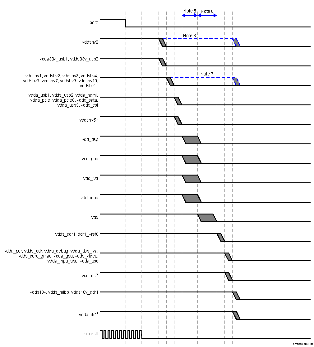 Figure 5-3 Power-Down Sequencing
 - xi_osc0 can be turned off anytime after porz assertion and must be turned off before vdda_osc voltage rail is shutdown.
- Grey shaded areas are windows where it is valid to ramp the voltage rail.
- Blue dashed lines are not valid windows but show alternate ramp possibilities based on the associated note.
- If RTC-mode is supported then vdda_rtc, vdd_rtc and vddshv5 must be individually powered with separate power supplies and cannot be combined with other rails.
- vdd_mpu, vdd_gpu, vdd_dsp, vdd_iva can be ramped at the same time or can be staggered.
- vdd must ramp after or at the same time as vdd_mpu, vdd_gpu, vdd_dsp and vdd_iva.
- If any of the vddshv[1-7,9-11] rails (not including vddshv8) are used as 1.8V only, then these rails can be combined with vdds18v. vddshv[1-7,9-11] is allowed to ramp down at either of the two points shown in the timing diagram in either 1.8V mode or in 3.3V mode. If vddshv[1-7,9-11] ramps down at the later time in the diagram then the board design must guarantee that the vddshv[1-7,9-11] rail is never higher than 2.0 V above the vdds18v rail.
- vddshv8 is separated out to show support for dual voltage. If a dedicated LDO/supply source is used for vddshv8, then vddshv8 ramp down should occur at one of the two earliest points in the timing diagram. If vddshv8 is powered by the same supply source as the other vddshvn rails, then it is allowed to ramp down at either of the last two points in the timing diagram.
Figure 5-4 describes the RTC-mode Power Sequencing.
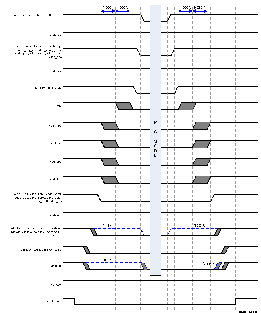 Figure 5-4 RTC Mode Sequencing
 - Grey shaded areas are windows where it is valid to ramp the voltage rail.
- Blue dashed lines are not valid windows but show alternate ramp possibilities based on the associated note.
- vdd must ramp down after or at the same time as vdd_mpu, vdd_gpu, vdd_dsp and vdd_iva.
- vdd_mpu, vdd_gpu, vdd_dsp, vdd_iva can be ramped at the same time or can be staggered.
- vdd must ramp up before or at the same time as vdd_mpu, vdd_gpu, vdd_dsp and vdd_iva.
- If any of the vddshv[1-7,9-11] rails (not including vddshv8) are used as 1.8V only, then these rails can be combined with vdds18v.
- vddshv8 is separated out to show support for dual voltage. If single voltage is used then vddshv8 can be combined with other vddshvn rails but vddshv8 must ramp down before vdd and must ramp up after vdd.
- If any of the vddshv[1-7,9-11] rails (not including vddshv8) are used as 1.8V only, then these rails can be combined with vdds18v. vddshv[1-7,9-11] is allowed to ramp down at either of the two points shown in the timing diagram in either 1.8V mode or in 3.3V mode. If vddshv[1-7,9-11] ramps down at the later time in the diagram then the board design must guarantee that the vddshvn rail is never higher than 2.0 V above the vdds18v rail.
- vddshv8 is separated out to show support for dual voltage. If a dedicated LDO/supply source is used for vddshv8, then vddshv8 ramp down should occur at one of the two earliest points in the timing diagram. If vddshv8 is powered by the same supply source as the other vddshvn rails, then it is allowed to ramp down at either of the last two points in the timing diagram.
Figure 5-5 and Figure 5-6 describe the device Power Sequencing when RTC-mode is NOT used.
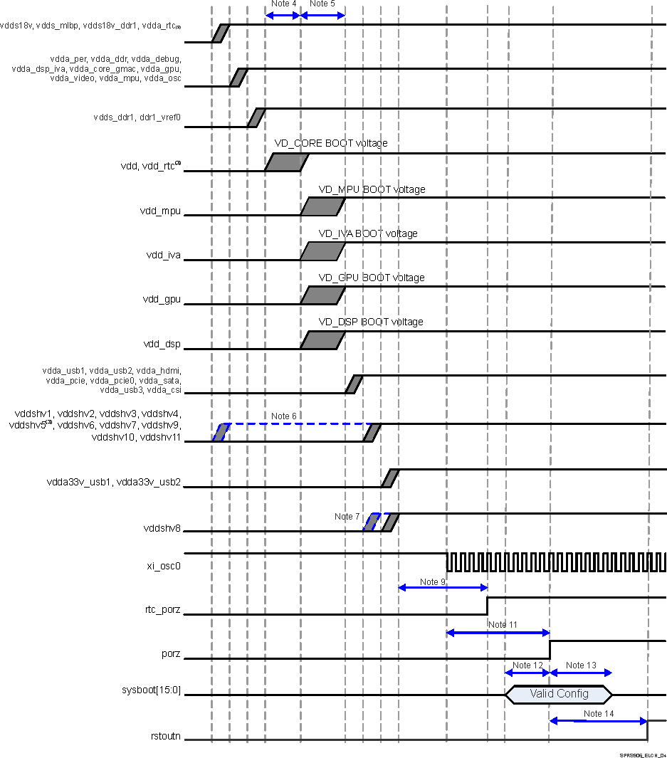 Figure 5-5 Power-Up Sequencing
 - Grey shaded areas are windows where it is valid to ramp the voltage rail.
- Blue dashed lines are not valid windows but show alternate ramp possibilities based on the associated note.
- If RTC-mode is not supported then the following combinations are approved:
- vdda_rtc can be combined with vdds18v
- vdd_rtc can be combined with vdd
- vddshv5 can be combined with other 1.8V or 3.3V vddshvn rails.
If combinations listed above are not followed then sequencing for these 3 voltage rails should follow the RTC mode timing requirements. - vdd must ramp before or at the same time as vdd_mpu, vdd_gpu, vdd_dsp and vdd_iva.
- vdd_mpu, vdd_gpu, vdd_dsp, vdd_iva can be ramped at the same time or can be staggered.
- If any of the vddshv[1-7,9-11] rails (not including vddshv8) are used as 1.8V only, then these rails can be combined with vdds18v.
- vddshv8 is separated out to show support for dual voltage. If single voltage is used then vddshv8 can be combined with other vddshvn rails but vddshv8 must ramp after vdd.
- vdds and vdda rails must not be combined together, with the one exception of vdda_rtc when RTC-mode is not supported.
- Pulse duration: rtc_porz must remain low 1ms after vdda_rtc, vddshv5, and vdd_rtc are ramped and stable.
- The SYS_32K source must be stable and at a valid frequency 1ms prior to de-asserting rtc_porz high.
- Pulse duration: porz must remain low a minimum of 12P(15) after xi_osc0 is stable and at a valid frequency. porz must also remain low until all supply rails are valid and stable. resetn must be high prior to, or simultaneous with, porz rising. During initial power-up, resetn can rise any time after, or concurrently with, its supply voltage, vddshv3 rising.
- Setup time: sysboot[15:0] pins must be valid 2P(15) before porz is de-asserted high.
- Hold time: sysboot[15:0] pins must be valid 15P(15) after porz is de-asserted high.
- porz to rstoutn delay is 2ms.
- P = 1/(SYS_CLK1/610) frequency in ns.
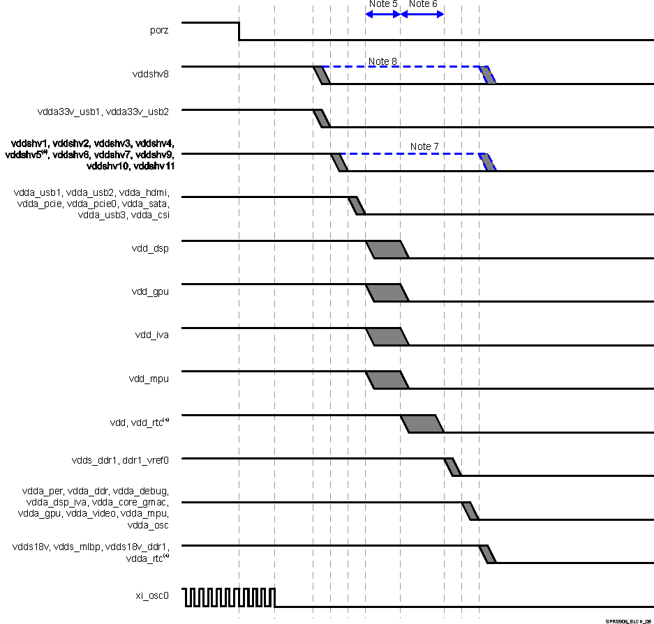 Figure 5-6 Power-Down Sequencing
 - Grey shaded areas are windows where it is valid to ramp the voltage rail.
- Blue dashed lines are not valid windows but show alternate ramp possibilities based on the associated note.
- xi_osc0 can be turned off anytime after porz assertion and must be turned off before vdda_osc voltage rail is shutdown.
- If RTC-mode is not used then the following combinations are approved:
- vdda_rtc can be combined with vdds18v
- vdd_rtc can be combined with vdd
- vddshv5 can be combined with other 1.8V or 3.3V vddshvn rails
If combinations listed above are not followed then sequencing for these 3 voltage rails should follow the RTC mode timing requirements. - vdd_mpu, vdd_gpu, vdd_dsp, vdd_iva can be ramped at the same time or can be staggered.
- vdd must ramp after or at the same time as vdd_mpu, vdd_gpu, vdd_dsp and vdd_iva.
- If any of the vddshv[1-7,9-11] rails (not including vddshv8) are used as 1.8V only, then these rails can be combined with vdds18v. vddshv[1-7,9-11] is allowed to ramp down at either of the two points shown in the timing diagram in either 1.8V mode or in 3.3V mode. If vddshv[1-7,9-11] ramps down at the later time in the diagram then the board design must guarantee that the vddshv[1-7,9-11] rail is never higher than 2.0 V above the vdds18v rail.
- vddshv8 is separated out to show support for dual voltage. If a dedicated LDO/supply source is used for vddshv8, then vddshv8 ramp down should occur at one of the two earliest points in the timing diagram. If vddshv8 is powered by the same supply source as the other vddshvn rails, then it is allowed to ramp down at either of the last two points in the timing diagram.
Figure 5-7 describes vddshv[1-7,9-11] Supplies Falling Before vdds18v Supplies Delta.
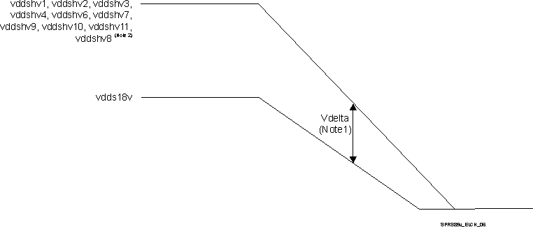 Figure 5-7 vddshv* Supplies Falling After vdds18v Supplies Delta
 - Vdelta MAX = 2V
- If vddshv8 is powered by the same supply source as the other vddshv[1-7,9-11] rails.