ZHCSJC6F March 2016 – June 2018 TDA2E
PRODUCTION DATA.
- 1 器件概述
- 2 修订历史记录
- 3 Device Comparison
-
4 Terminal Configuration and Functions
- 4.1 Terminal Assignment
- 4.2 Ball Characteristics
- 4.3 Multiplexing Characteristics
- 4.4
Signal Descriptions
- 4.4.1 Video Input Ports (VIP)
- 4.4.2 Display Subsystem – Video Output Ports
- 4.4.3 Display Subsystem – High-Definition Multimedia Interface (HDMI)
- 4.4.4 Camera Serial Interface 2 CAL bridge (CSI2)
- 4.4.5 External Memory Interface (EMIF SDRAM)
- 4.4.6 General-Purpose Memory Controller (GPMC)
- 4.4.7 Timers
- 4.4.8 Inter-Integrated Circuit Interface (I2C)
- 4.4.9 Universal Asynchronous Receiver Transmitter (UART)
- 4.4.10 Multichannel Serial Peripheral Interface (McSPI)
- 4.4.11 Quad Serial Peripheral Interface (QSPI)
- 4.4.12 Multichannel Audio Serial Port (McASP)
- 4.4.13 Universal Serial Bus (USB)
- 4.4.14 SATA
- 4.4.15 Peripheral Component Interconnect Express (PCIe)
- 4.4.16 Controller Area Network Interface (DCAN)
- 4.4.17 Ethernet Interface (GMAC_SW)
- 4.4.18 eMMC/SD/SDIO
- 4.4.19 General-Purpose Interface (GPIO)
- 4.4.20 Pulse Width Modulation (PWM) Interface
- 4.4.21 Test Interfaces
- 4.4.22 System and Miscellaneous
- 4.4.23 Power Supplies
-
5 Specifications
- 5.1 Absolute Maximum Ratings
- 5.2 ESD Ratings
- 5.3 Power on Hour (POH) Limits
- 5.4 Recommended Operating Conditions
- 5.5 Operating Performance Points
- 5.6 Power Consumption Summary
- 5.7
Electrical Characteristics
- 5.7.1 LVCMOS DDR DC Electrical Characteristics
- 5.7.2 HDMIPHY DC Electrical Characteristics
- 5.7.3 Dual Voltage LVCMOS I2C DC Electrical Characteristics
- 5.7.4 IQ1833 Buffers DC Electrical Characteristics
- 5.7.5 IHHV1833 Buffers DC Electrical Characteristics
- 5.7.6 LVCMOS CSI2 DC Electrical Characteristics
- 5.7.7 BC1833IHHV Buffers DC Electrical Characteristics
- 5.7.8 USBPHY DC Electrical Characteristics
- 5.7.9 Dual Voltage SDIO1833 DC Electrical Characteristics
- 5.7.10 Dual Voltage LVCMOS DC Electrical Characteristics
- 5.7.11 SATAPHY DC Electrical Characteristics
- 5.7.12 PCIEPHY DC Electrical Characteristics
- 5.8 Thermal Characteristics
- 5.9 Power Supply Sequences
- 6 Clock Specifications
-
7 Timing Requirements and Switching Characteristics
- 7.1 Timing Test Conditions
- 7.2 Interface Clock Specifications
- 7.3 Timing Parameters and Information
- 7.4 Recommended Clock and Control Signal Transition Behavior
- 7.5 Virtual and Manual I/O Timing Modes
- 7.6 Video Input Ports (VIP)
- 7.7 Display Subsystem - Video Output Ports
- 7.8 Display Subsystem - High-Definition Multimedia Interface (HDMI)
- 7.9 Camera Serial Interface 2 CAL bridge (CSI2)
- 7.10 External Memory Interface (EMIF)
- 7.11 General-Purpose Memory Controller (GPMC)
- 7.12 Timers
- 7.13 Inter-Integrated Circuit Interface (I2C)
- 7.14 Universal Asynchronous Receiver Transmitter (UART)
- 7.15 Multichannel Serial Peripheral Interface (McSPI)
- 7.16 Quad Serial Peripheral Interface (QSPI)
- 7.17 Multichannel Audio Serial Port (McASP)
- 7.18 Universal Serial Bus (USB)
- 7.19 Serial Advanced Technology Attachment (SATA)
- 7.20 Peripheral Component Interconnect Express (PCIe)
- 7.21 Controller Area Network Interface (DCAN)
- 7.22
Ethernet Interface (GMAC_SW)
- 7.22.1
GMAC MII Timings
- Table 7-66 Timing Requirements for miin_rxclk - MII Operation
- Table 7-67 Timing Requirements for miin_txclk - MII Operation
- Table 7-68 Timing Requirements for GMAC MIIn Receive 10/100 Mbit/s
- Table 7-69 Switching Characteristics Over Recommended Operating Conditions for GMAC MIIn Transmit 10/100 Mbits/s
- 7.22.2 GMAC MDIO Interface Timings
- 7.22.3
GMAC RMII Timings
- Table 7-74 Timing Requirements for GMAC REF_CLK - RMII Operation
- Table 7-75 Timing Requirements for GMAC RMIIn Receive
- Table 7-76 Switching Characteristics Over Recommended Operating Conditions for GMAC REF_CLK - RMII Operation
- Table 7-77 Switching Characteristics Over Recommended Operating Conditions for GMAC RMIIn Transmit 10/100 Mbits/s
- 7.22.4
GMAC RGMII Timings
- Table 7-81 Timing Requirements for rgmiin_rxc - RGMIIn Operation
- Table 7-82 Timing Requirements for GMAC RGMIIn Input Receive for 10/100/1000 Mbps
- Table 7-83 Switching Characteristics Over Recommended Operating Conditions for rgmiin_txctl - RGMIIn Operation for 10/100/1000 Mbit/s
- Table 7-84 Switching Characteristics for GMAC RGMIIn Output Transmit for 10/100/1000 Mbps
- 7.22.1
GMAC MII Timings
- 7.23
eMMC/SD/SDIO
- 7.23.1
MMC1-SD Card Interface
- 7.23.1.1 Default speed, 4-bit data, SDR, half-cycle
- 7.23.1.2 High speed, 4-bit data, SDR, half-cycle
- 7.23.1.3 SDR12, 4-bit data, half-cycle
- 7.23.1.4 SDR25, 4-bit data, half-cycle
- 7.23.1.5 UHS-I SDR50, 4-bit data, half-cycle
- 7.23.1.6 UHS-I SDR104, 4-bit data, half-cycle
- 7.23.1.7 UHS-I DDR50, 4-bit data
- 7.23.2 MMC2 - eMMC
- 7.23.3 MMC3 and MMC4-SDIO/SD
- 7.23.1
MMC1-SD Card Interface
- 7.24 General-Purpose Interface (GPIO)
- 7.25 System and Miscellaneous interfaces
- 7.26
Test Interfaces
- 7.26.1
IEEE 1149.1 Standard-Test-Access Port (JTAG)
- 7.26.1.1
JTAG Electrical Data/Timing
- Table 7-131 Timing Requirements for IEEE 1149.1 JTAG
- Table 7-132 Switching Characteristics Over Recommended Operating Conditions for IEEE 1149.1 JTAG
- Table 7-133 Timing Requirements for IEEE 1149.1 JTAG With RTCK
- Table 7-134 Switching Characteristics Over Recommended Operating Conditions for IEEE 1149.1 JTAG With RTCK
- 7.26.1.1
JTAG Electrical Data/Timing
- 7.26.2 Trace Port Interface Unit (TPIU)
- 7.26.1
IEEE 1149.1 Standard-Test-Access Port (JTAG)
-
8 Applications, Implementation, and Layout
- 8.1 Introduction
- 8.2 Power Optimizations
- 8.3 Core Power Domains
- 8.4 Single-Ended Interfaces
- 8.5
Differential Interfaces
- 8.5.1 General Routing Guidelines
- 8.5.2
USB 2.0 Board Design and Layout Guidelines
- 8.5.2.1 Background
- 8.5.2.2
USB PHY Layout Guide
- 8.5.2.2.1 General Routing and Placement
- 8.5.2.2.2
Specific Guidelines for USB PHY Layout
- 8.5.2.2.2.1 Analog, PLL, and Digital Power Supply Filtering
- 8.5.2.2.2.2 Analog, Digital, and PLL Partitioning
- 8.5.2.2.2.3 Board Stackup
- 8.5.2.2.2.4 Cable Connector Socket
- 8.5.2.2.2.5 Clock Routings
- 8.5.2.2.2.6 Crystals/Oscillator
- 8.5.2.2.2.7 DP/DM Trace
- 8.5.2.2.2.8 DP/DM Vias
- 8.5.2.2.2.9 Image Planes
- 8.5.2.2.2.10 Power Regulators
- 8.5.2.3 References
- 8.5.3 USB 3.0 Board Design and Layout Guidelines
- 8.5.4 HDMI Board Design and Layout Guidelines
- 8.5.5 PCIe Board Design and Layout Guidelines
- 8.5.6 CSI2 Board Design and Routing Guidelines
- 8.6
DDR3 Board Design and Layout Guidelines
- 8.6.1 DDR3 General Board Layout Guidelines
- 8.6.2
DDR3 Board Design and Layout Guidelines
- 8.6.2.1 Board Designs
- 8.6.2.2 DDR3 EMIF
- 8.6.2.3 DDR3 Device Combinations
- 8.6.2.4 DDR3 Interface Schematic
- 8.6.2.5 Compatible JEDEC DDR3 Devices
- 8.6.2.6 PCB Stackup
- 8.6.2.7 Placement
- 8.6.2.8 DDR3 Keepout Region
- 8.6.2.9 Bulk Bypass Capacitors
- 8.6.2.10 High-Speed Bypass Capacitors
- 8.6.2.11 Net Classes
- 8.6.2.12 DDR3 Signal Termination
- 8.6.2.13 VREF_DDR Routing
- 8.6.2.14 VTT
- 8.6.2.15 CK and ADDR_CTRL Topologies and Routing Definition
- 8.6.2.16 Data Topologies and Routing Definition
- 8.6.2.17 Routing Specification
- 9 Device and Documentation Support
- 10Mechanical Packaging Information
8.6.2.15.1.2 CK and ADDR_CTRL Routing, Four DDR3 Devices
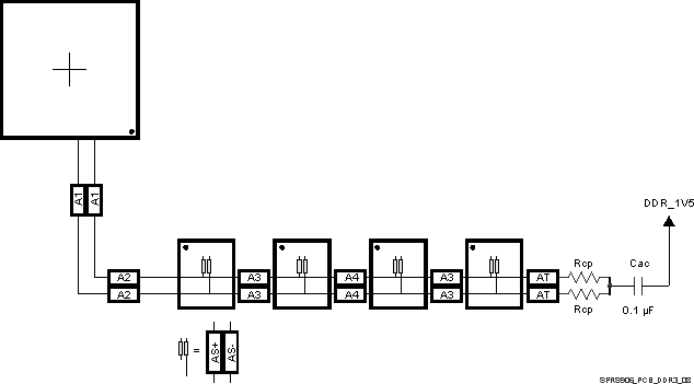
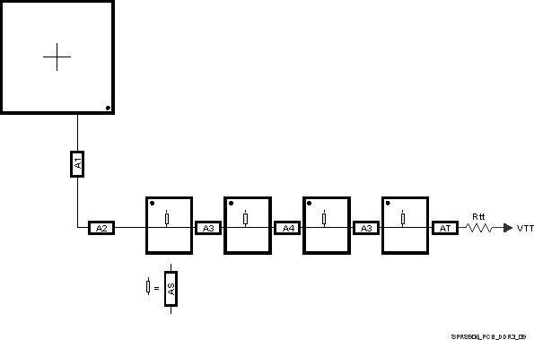
Figure 8-43 shows the CK routing for four DDR3 devices placed on the same side of the PCB. Figure 8-44 shows the corresponding ADDR_CTRL routing.
 Figure 8-43 CK Routing for Four Single-Side DDR3 Devices
  Figure 8-44 ADDR_CTRL Routing for Four Single-Side DDR3 Devices
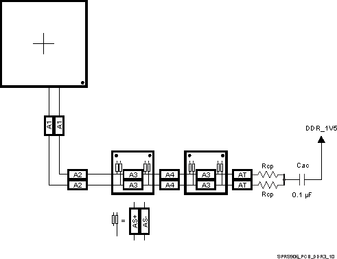
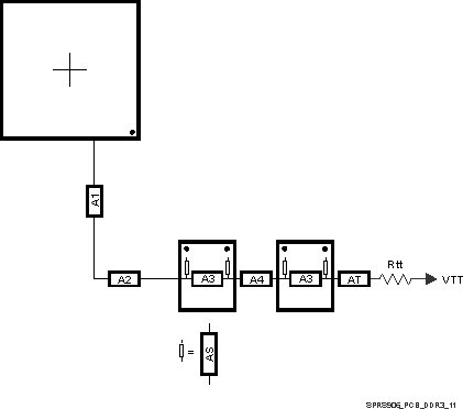
 To save PCB space, the four DDR3 memories may be mounted as two mirrored pairs at a cost of increased routing and assembly complexity. Figure 8-45 and Figure 8-46 show the routing for CK and ADDR_CTRL, respectively, for four DDR3 devices mirrored in a two-pair configuration.
 Figure 8-45 CK Routing for Four Mirrored DDR3 Devices
  Figure 8-46 ADDR_CTRL Routing for Four Mirrored DDR3 Devices