ZHCSNH1C May 2021 – November 2022 DLPC6540
PRODUCTION DATA
- 1 特性
- 2 应用
- 3 说明
- 4 Revision History
- 5 Pin Configuration and Functions
-
6 Specifications
- 6.1 Absolute Maximum Ratings
- 6.2 ESD Ratings
- 6.3 Recommended Operating Conditions
- 6.4 Thermal Information
- 6.5 Power Electrical Characteristics
- 6.6 Pin Electrical Characteristics
- 6.7 DMD HSSI Electrical Characteristics
- 6.8 DMD Low-Speed LVDS Electrical Characteristics
- 6.9 V-by-One Interface Electrical Characteristics
- 6.10 USB Electrical Characteristics
- 6.11 System Oscillator Timing Requirements
- 6.12 Power Supply and Reset Timing Requirements
- 6.13 DMD HSSI Timing Requirements
- 6.14 DMD Low-Speed LVDS Timing Requirements
- 6.15 V-by-One Interface General Timing Requirements
- 6.16 Source Frame Timing Requirements
- 6.17 Synchronous Serial Port Interface Timing Requirements
- 6.18 Master and Slave I2C Interface Timing Requirements
- 6.19 Programmable Output Clock Timing Requirements
- 6.20 JTAG Boundary Scan Interface Timing Requirements (Debug Only)
- 6.21 JTAG ARM Multi-Ice Interface Timing Requirements (Debug Only)
- 6.22 Multi-Trace ETM Interface Timing Requirements
- 7 Detailed Description
- 8 Power Supply Recommendations
-
9 Layout
- 9.1
Layout Guidelines
- 9.1.1 General Layout Guidelines
- 9.1.2 Power Supply Layout Guidelines
- 9.1.3 Layout Guidelines for Internal Controller PLL Power
- 9.1.4 Layout Guideline for DLPC6540 Reference Clock
- 9.1.5 V-by-One Interface Layout Considerations
- 9.1.6 USB Interface Layout Considerations
- 9.1.7 DMD Interface Layout Considerations
- 9.1.8 General Handling Guidelines for Unused CMOS-Type Pins
- 9.1.9 Maximum Pin-to-Pin, PCB Interconnects Etch Lengths
- 9.2 Thermal Considerations
- 9.1
Layout Guidelines
- 10Device and Documentation Support
- 11Mechanical, Packaging, and Orderable Information
6.10 USB Electrical Characteristics
Over operating free-air temperature range (unless otherwise noted)
| PARAMETER(1)(2) | MIN | NOM | MAX | UNIT | ||
|---|---|---|---|---|---|---|
| Low-Speed and Full Speed (Input Level) | ||||||
| VIH | Single-ended input voltage high (driven) | 2.0 | V | |||
| VIHZ | Single-ended input voltage high (floating) | 2.7 | 3.6 | V | ||
| VIL | Single-ended input voltage low | 0.8 | V | |||
| VDI | Differential input sensitivity | |(DP) - (DM)| | 0.2 | V | ||
| VCM | Differential common mode voltage | Includes VDI range | 0.8 | 2.5 | V | |
| Low-Speed and Full Speed (Output Level) | ||||||
| VOL | Low-level output voltage | with 1.425 KΩ pullup to 3.6 V | 0.0 | 0.3 | V | |
| VOH | High-level output voltage | with 14.25 KΩ pulldown | 2.8 | 3.6 | V | |
| VCRS | Output signal crossover voltage | 1.3 | 2.0 | V | ||
| High-Speed (Input Level) | ||||||
| VHSSQ | High-speed squelch detection threshold (differential signal amplitude) | 100 | 150 | mV | ||
| VHSDSC | High-speed disconnect detection threshold (differential signal amplitude) | 525 | 626 | mV | ||
| VHSCM | High-speed data signal common mode voltage | -50 | 500 | mV | ||
| High-Speed (Output Level) | ||||||
| VHSOI | High-speed idle level | –10.0 | 10.0 | mV | ||
| VHSOH | High-speed data signal - high | 360 | 440 | mV | ||
| VHSOL | High-speed data signal - low | –10.0 | 10.0 | mV | ||
| VCHIRPJ | High-speed chirp J level (differential voltage) | 700 | 1100 | mV | ||
| VCHIRPK | High-speed chirp K level (differential voltage) | -900 | -500 | mV | ||
| Termination | ||||||
| RPU | Bus pullup resistor | 1.425 | 1.575 | KΩ | ||
| RPD | Bus pulldown resistor | 14.25 | 15.75 | KΩ | ||
| ZHSDRV | High-speed driver output impedance | 40.5 | 49.5 | Ω | ||
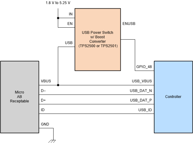
(1) Referenced to VAD33_USB (I/O type 11)
(2) When used as a master as part of USB OTG, the DLPC6540 requires an
external
USB
switch
to provide the USB 5-V power. The example shown in Figure 6-3
uses
a
TI TPS2500/2501 device. The example figure does not describe the required
ancillary components (such
as
resistors and capacitors). For this information,
refer
to the
USB
switch logic data
sheet for the selected device. The
external
USB
switch
is not required for product configurations that
support
USB slave mode only.
 Figure 6-3 External USB Switch Example for DLPC6540 Controller as USB OTG Master