ZHCSNH1C May 2021 – November 2022 DLPC6540
PRODUCTION DATA
- 1 特性
- 2 应用
- 3 说明
- 4 Revision History
- 5 Pin Configuration and Functions
-
6 Specifications
- 6.1 Absolute Maximum Ratings
- 6.2 ESD Ratings
- 6.3 Recommended Operating Conditions
- 6.4 Thermal Information
- 6.5 Power Electrical Characteristics
- 6.6 Pin Electrical Characteristics
- 6.7 DMD HSSI Electrical Characteristics
- 6.8 DMD Low-Speed LVDS Electrical Characteristics
- 6.9 V-by-One Interface Electrical Characteristics
- 6.10 USB Electrical Characteristics
- 6.11 System Oscillator Timing Requirements
- 6.12 Power Supply and Reset Timing Requirements
- 6.13 DMD HSSI Timing Requirements
- 6.14 DMD Low-Speed LVDS Timing Requirements
- 6.15 V-by-One Interface General Timing Requirements
- 6.16 Source Frame Timing Requirements
- 6.17 Synchronous Serial Port Interface Timing Requirements
- 6.18 Master and Slave I2C Interface Timing Requirements
- 6.19 Programmable Output Clock Timing Requirements
- 6.20 JTAG Boundary Scan Interface Timing Requirements (Debug Only)
- 6.21 JTAG ARM Multi-Ice Interface Timing Requirements (Debug Only)
- 6.22 Multi-Trace ETM Interface Timing Requirements
- 7 Detailed Description
- 8 Power Supply Recommendations
-
9 Layout
- 9.1
Layout Guidelines
- 9.1.1 General Layout Guidelines
- 9.1.2 Power Supply Layout Guidelines
- 9.1.3 Layout Guidelines for Internal Controller PLL Power
- 9.1.4 Layout Guideline for DLPC6540 Reference Clock
- 9.1.5 V-by-One Interface Layout Considerations
- 9.1.6 USB Interface Layout Considerations
- 9.1.7 DMD Interface Layout Considerations
- 9.1.8 General Handling Guidelines for Unused CMOS-Type Pins
- 9.1.9 Maximum Pin-to-Pin, PCB Interconnects Etch Lengths
- 9.2 Thermal Considerations
- 9.1
Layout Guidelines
- 10Device and Documentation Support
- 11Mechanical, Packaging, and Orderable Information
9.1.4.1 Recommended Crystal Oscillator Configuration
Table 9-2 Recommended Crystal
Configurations
| PARAMETER | CRYSTAL A | CRYSTAL B | UNIT |
|---|---|---|---|
| Crystal circuit configuration | Parallel resonant | Parallel resonant | |
| Crystal type | Fundamental (first harmonic) | Fundamental (first harmonic) | |
| Crystal nominal frequency | 40 | 38 | MHz |
| Crystal frequency tolerance (1) | ±100 (200 p-p max) | ±100 (200 p-p max) | PPM |
| Crystal equivalent series resistance (ESR) | 60 (Max) | 60 (Max) | Ω |
| Crystal load capacitance | 20 (Max) | 20 (Max) | pF |
| Crystal Shunt Load capacitance | 7 (Max) | 7 (Max) | pF |
| Temperature range | –40°C to +85°C | –40°C to +85°C | °C |
| Drive level | 100 (Nominal) | 100 (Nominal) | µW |
| RFB feedback resistor (nominal) | 1 Meg (Nominal) | 1 Meg (Nominal) | Ω |
| CL1 external crystal load capacitor | See equation in (2). | See equation in (2). | pF |
| CL2 external crystal load capacitor | See equation in (3). | See equation in (3). | pF |
| PCB layout | A ground isolation ring around the crystal is recommended. | A ground isolation ring around the crystal is recommended. |
(1) Crystal frequency tolerance to include accuracy, temperature, aging,
and trim sensitivity. These are typically specified separately and the sum of
all required to meet this requirement.
(2) CL1 = 2 × (CL – Cstray_pll_refclk_i), where: Cstray_pll_refclk_i =
Sum of package and PCB stray capacitance at the crystal pin associated with the
Controller pin REFCLKx_I. See Table 9-3.
(3) CL2 = 2 × (CL – Cstray_pll_refclk_o), where: Cstray_pll_refclk_o =
Sum of package and PCB stray capacitance at the crystal pin associated with the
Controller pin REFCLKx_O. See Table 9-3.
Table 9-3 Crystal Pin
Capacitance
| PARAMETER | MIN | NOM | MAX | UNITS | |
|---|---|---|---|---|---|
| Cstray_pll_refclkA_i | Sum of package and PCB stray capacitance at REFCLKA_I | 4.5 | pF | ||
| Cstray_pll_refclkA_o | Sum of package and PCB stray capacitance at REFCLKA_O | 4.5 | pF | ||
| Cstray_pll_refclkB_i | Sum of package and PCB stray capacitance at REFCLKB_I | 4.5 | pF | ||
| Cstray_pll_refclkB_o | Sum of package and PCB stray capacitance at REFCLKB_O | 4.5 | pF | ||
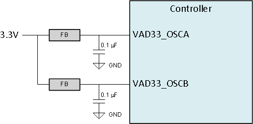
The crystal circuits in the DLPC6540 have dedicated power (VAD33_OSCA and VAD33_OSCB) pins, with the recommended filtering for each shown in Figure 9-11, and recommended values shown in Table 9-1.
 Figure 9-11 Crystal
Power Supply Filtering
Figure 9-11 Crystal
Power Supply FilteringTable 9-4 DLPC6540
Recommended Crystal Parts
| MANUFACTURER | PART NUMBER | NOMINAL FREQUENCY | FREQUENCY
TOLERANCE, FREQUENCY STABILITY, AGING/YEAR |
ESR | LOAD CAPACITANCE | OPERATING TEMPERATURE | DRIVE LEVEL |
|---|---|---|---|---|---|---|---|
| TXC | 7M38070001 (1) | 38 MHz | Freq Tolerance: ±20 ppm |
30-Ω max | 12 pF | –40°C to +85°C | 100 µW |
| Freq Stability: ±20 ppm |
|||||||
| Aging/Year: ±3 ppm | |||||||
| TXC | 7M40070041 (2) | 40 MHz | Freq Tolerance: ±20 ppm |
30-Ω max | 12 pF | –40°C to +85°C | 100 µW |
| Freq Stability: ±20 ppm |
|||||||
| Aging/Year: ±3 ppm |
(1) This device requires an RS resistor with value = 0.
(2) This device requires an RS resistor with value = 0.