ZHCSNH1C May 2021 – November 2022 DLPC6540
PRODUCTION DATA
- 1 特性
- 2 应用
- 3 说明
- 4 Revision History
- 5 Pin Configuration and Functions
-
6 Specifications
- 6.1 Absolute Maximum Ratings
- 6.2 ESD Ratings
- 6.3 Recommended Operating Conditions
- 6.4 Thermal Information
- 6.5 Power Electrical Characteristics
- 6.6 Pin Electrical Characteristics
- 6.7 DMD HSSI Electrical Characteristics
- 6.8 DMD Low-Speed LVDS Electrical Characteristics
- 6.9 V-by-One Interface Electrical Characteristics
- 6.10 USB Electrical Characteristics
- 6.11 System Oscillator Timing Requirements
- 6.12 Power Supply and Reset Timing Requirements
- 6.13 DMD HSSI Timing Requirements
- 6.14 DMD Low-Speed LVDS Timing Requirements
- 6.15 V-by-One Interface General Timing Requirements
- 6.16 Source Frame Timing Requirements
- 6.17 Synchronous Serial Port Interface Timing Requirements
- 6.18 Master and Slave I2C Interface Timing Requirements
- 6.19 Programmable Output Clock Timing Requirements
- 6.20 JTAG Boundary Scan Interface Timing Requirements (Debug Only)
- 6.21 JTAG ARM Multi-Ice Interface Timing Requirements (Debug Only)
- 6.22 Multi-Trace ETM Interface Timing Requirements
- 7 Detailed Description
- 8 Power Supply Recommendations
-
9 Layout
- 9.1
Layout Guidelines
- 9.1.1 General Layout Guidelines
- 9.1.2 Power Supply Layout Guidelines
- 9.1.3 Layout Guidelines for Internal Controller PLL Power
- 9.1.4 Layout Guideline for DLPC6540 Reference Clock
- 9.1.5 V-by-One Interface Layout Considerations
- 9.1.6 USB Interface Layout Considerations
- 9.1.7 DMD Interface Layout Considerations
- 9.1.8 General Handling Guidelines for Unused CMOS-Type Pins
- 9.1.9 Maximum Pin-to-Pin, PCB Interconnects Etch Lengths
- 9.2 Thermal Considerations
- 9.1
Layout Guidelines
- 10Device and Documentation Support
- 11Mechanical, Packaging, and Orderable Information
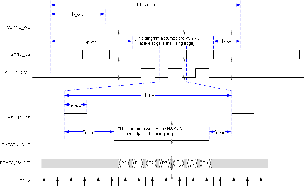
6.16 Source Frame Timing Requirements
See Figure 6-14
| PARAMETER (1) | MIN | MAX | UNIT | ||
|---|---|---|---|---|---|
| tp_vsw | VSYNC Active Pulse Width | 50% reference points | 1 | 127 | lines |
| tp_vbp | Vertical back porch (VBP) (2) | 50% reference points | 2 (3) | lines | |
| tp_vƒp | Vertical front porch (VFP) (2) | 50% reference points | MAX[ (TVBMIN - 65 ), 1] (3) | lines | |
| tp_tvb | Total vertical blanking (TVB) (2) | 50% reference points | See (4) | lines | |
| tp_hsw | HSYNC Active Pulse Width | 50% reference points | 16 | PCLKs | |
| tp_hbp | Horizontal back porch (HBP) (5) | 50% reference points | 5 (Digital Video Sources) 65 (Analog Video Sources) | PCLKs | |
| tp_hfp | Horizontal front porch (HFP) (5) | 50% reference points | 2 | PCLKs | |
| tp_thb | Total horizontal blanking (THB) (5) | 50% reference points | 20 (Digital Video Sources) 80 (Analog Video Sources) (6) | PCLKs | |
| fline | Horizontal line rate | 37.354 | K Hz | ||
| APPL | Active Pixels per Line | 640 | 4096 | Pixels | |
| ALPF | Active Lines per Frame | 480 | 2160 (Normal) | Lines | |
(1) The requirements in the table apply to all external sources
(2) Vertical Blanking Parameter Definitions:
- Vertical Back Porch: Time from the leading edge of VSYNC to the leading edge of HSYNC for the first active line, and includes the VSYNC pulse width tp_vsw.
- Vertical Front Porch: Time from the leading edge of HSYNC following the last active line in a frame to the leading edge of VSYNC
- Total Vertical Blanking: The sum of VBP + VFP = TVB.
(3) The vertical blanking required (per TVB) can be allocated as desired
as long as the VFP and VBP minimum values are met.
(4) The minimum TVB can be calculated using the following:
TVBmin = 11 + ROUNDUP(LLS_VFP_MIN × (Source_ALPF/VPS_ALPF)), where:
TVBmin = 11 + ROUNDUP(LLS_VFP_MIN × (Source_ALPF/VPS_ALPF)), where:
- LLS_VFP_MIN (Normal Mode) = 22
- Source_ALPF = Active Lines Per Frame of the incoming source
- VPS_ALPF = 1080 (for 1920x1080 Native products and 3840x2160 4-way XPR products)
- Less TVBmin blanking can be required depending on the video processing being done. The configurations that drive the worst case minimum value are those configurations that combine the maximum (or near maximum) capabilities of functions such as scaling, warping, and keystone correction.
- This is applicable to all sources (Section 7.4). Other sources require directed testing in the end application.
- The minimum recommended TVB with CVT 1.2 sources is 23.
(5) Horizontal Blanking Parameter Definitions:
- Horizontal Back Porch: Time from the leading edge of HSYNC to the rising edge of DATEN, and includes the HSYNC pulse width tp_hsw.
- Horizontal Front Porch: Time from the falling edge of DATEN to the leading edge of HSYNC.
- Total Horizontal Blanking: The sum of HBP + HFP = THB.
(6) The horizontal blanking required (per THB) can be allocated as desired as long as the HFP and HBP minimum values are met.
 Figure 6-14 Source Frame Timing