ZHCSRK4A April 2020 – September 2020 CC2640R2L
PRODUCTION DATA
- 1 特性
- 2 应用
- 3 说明
- 4 Functional Block Diagram
- 5 Revision History
- 6 Device Comparison
- 7 Terminal Configuration and Functions
-
8 Specifications
- 8.1 Absolute Maximum Ratings
- 8.2 ESD Ratings
- 8.3 Recommended Operating Conditions
- 8.4 Power Consumption Summary
- 8.5 General Characteristics
- 8.6 125-kbps Coded (Bluetooth 5) – RX
- 8.7 125-kbps Coded (Bluetooth 5) – TX
- 8.8 500-kbps Coded (Bluetooth 5) – RX
- 8.9 500-kbps Coded (Bluetooth 5) – TX
- 8.10 1-Mbps GFSK (Bluetooth low energy) – RX
- 8.11 1-Mbps GFSK (Bluetooth low energy) – TX
- 8.12 2-Mbps GFSK (Bluetooth 5) – RX
- 8.13 2-Mbps GFSK (Bluetooth 5) – TX
- 8.14 24-MHz Crystal Oscillator (XOSC_HF)
- 8.15 32.768-kHz Crystal Oscillator (XOSC_LF)
- 8.16 48-MHz RC Oscillator (RCOSC_HF)
- 8.17 32-kHz RC Oscillator (RCOSC_LF)
- 8.18 ADC Characteristics
- 8.19 Temperature Sensor
- 8.20 Battery Monitor
- 8.21 Synchronous Serial Interface (SSI)
- 8.22 DC Characteristics
- 8.23 Thermal Resistance Characteristics
- 8.24 Timing Requirements
- 8.25 Switching Characteristics
- 8.26 Typical Characteristics
- 9 Detailed Description
- 10Application, Implementation, and Layout
- 11Device and Documentation Support
- 12Mechanical, Packaging, and Orderable Information
封装选项
机械数据 (封装 | 引脚)
散热焊盘机械数据 (封装 | 引脚)
订购信息
8.21 Synchronous Serial Interface (SSI)
Tc = 25°C, VDDS = 3.0 V, unless otherwise noted.
| PARAMETER | TEST CONDITIONS | MIN | TYP | MAX | UNIT |
|---|---|---|---|---|---|
| S1#SWRS1584470 tclk_per (SSIClk period) | Device operating as slave | 12 | 65024 | system clocks | |
| S2#SWRS1584470 tclk_high (SSIClk high time) | Device operating as slave | 0.5 | tclk_per | ||
| S3#SWRS1584470 tclk_low (SSIClk low time) | Device operating as slave | 0.5 | tclk_per | ||
| S1 (TX only)#SWRS1584470 tclk_per (SSIClk period) | One-way communication to slave, device operating as master | 4 | 65024 | system clocks | |
| S1 (TX and RX)#SWRS1584470 tclk_per (SSIClk period) | Normal duplex operation, device operating as master | 8 | 65024 | system clocks | |
| S2#SWRS1584470 tclk_high (SSIClk high time) | Device operating as master | 0.5 | tclk_per | ||
| S3#SWRS1584470 tclk_low (SSIClk low time) | Device operating as master | 0.5 | tclk_per |
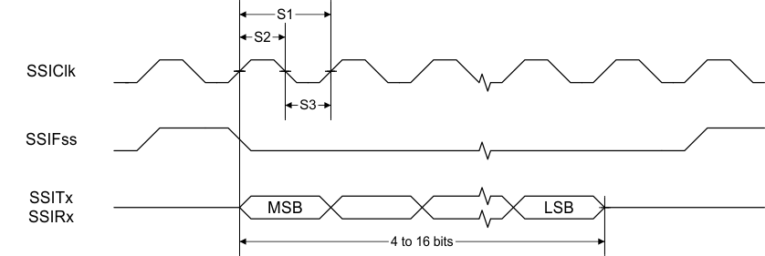
 Figure 8-1 SSI
Timing for TI Frame Format (FRF = 01), Single Transfer Timing
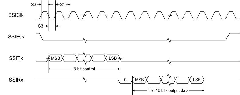
Measurement
 Figure 8-2 SSI
Timing for MICROWIRE Frame Format (FRF = 10), Single Transfer
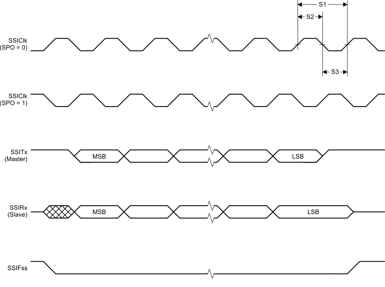
 Figure 8-3 SSI
Timing for SPI Frame Format (FRF = 00), With SPH = 1