ZHCSJY1A June   2019  – January 2021 ADS125H01

PRODUCTION DATA  

  1. 特性
  2. 应用
  3. 说明
  4. Revision History
  5. Device Comparison Table
  6. Pin Configuration and Functions
  7. Specifications
    1. 7.1 Absolute Maximum Ratings
    2. 7.2 ESD Ratings
    3. 7.3 Recommended Operating Conditions
    4. 7.4 Thermal Information
    5. 7.5 Electrical Characteristics
    6. 7.6 Timing Requirements
    7. 7.7 Switching Characteristics
    8. 7.8 Timing Diagrams
    9. 7.9 Typical Characteristics
  8. Parameter Measurement Information
    1. 8.1 Noise Performance
  9. Detailed Description
    1. 9.1 Overview
    2. 9.2 Functional Block Diagram
    3. 9.3 Feature Description
      1. 9.3.1 Input Voltage Range
      2. 9.3.2 Analog Inputs (AINP, AINN)
        1. 9.3.2.1 ESD Diodes
        2. 9.3.2.2 Input Switch
      3. 9.3.3 Programmable Gain Amplifier (PGA)
        1. 9.3.3.1 PGA Operating Range
        2. 9.3.3.2 PGA Monitors
      4. 9.3.4 Reference Voltage
        1. 9.3.4.1 Reference Monitor
      5. 9.3.5 ADC Modulator
      6. 9.3.6 Digital Filter
        1. 9.3.6.1 Sinc Filter Mode
          1. 9.3.6.1.1 Sinc Filter Frequency Response
        2. 9.3.6.2 FIR Filter
        3. 9.3.6.3 50-Hz and 60-Hz Normal-Mode Rejection
    4. 9.4 Device Functional Modes
      1. 9.4.1 Conversion Control
        1. 9.4.1.1 Continuous-Conversion Mode
        2. 9.4.1.2 Pulse-Conversion Mode
        3. 9.4.1.3 Conversion Latency
        4. 9.4.1.4 Start-Conversion Delay
      2. 9.4.2 Clock Mode
      3. 9.4.3 Reset
        1. 9.4.3.1 Power-On Reset
        2. 9.4.3.2 Reset by RESETPin
        3. 9.4.3.3 Reset by Command
      4. 9.4.4 Calibration
        1. 9.4.4.1 Offset and Full-Scale Calibration
          1. 9.4.4.1.1 Offset Calibration Registers
          2. 9.4.4.1.2 Full-Scale Calibration Registers
        2. 9.4.4.2 Offset Calibration Command (OFSCAL)
        3. 9.4.4.3 Full-Scale Calibration Command (GANCAL)
        4. 9.4.4.4 Calibration Command Procedure
        5. 9.4.4.5 User Calibration Procedure
    5. 9.5 Programming
      1. 9.5.1 Serial Interface
        1. 9.5.1.1 Chip-Select Pins (CS1 and CS2)
        2. 9.5.1.2 Serial Clock (SCLK)
        3. 9.5.1.3 Data Input (DIN)
        4. 9.5.1.4 Data Output/Data Ready (DOUT/DRDY)
      2. 9.5.2 Data Ready (DRDY)
        1. 9.5.2.1 DRDY in Continuous-Conversion Mode
        2. 9.5.2.2 DRDY in Pulse-Conversion Mode
        3. 9.5.2.3 Data Ready by Software Polling
      3. 9.5.3 Conversion Data
        1. 9.5.3.1 Status Byte (STATUS0)
        2. 9.5.3.2 Conversion Data Format
      4. 9.5.4 Cyclic Redundancy Check (CRC)
      5. 9.5.5 Commands
        1. 9.5.5.1  General Command Format
        2. 9.5.5.2  NOP Command
        3. 9.5.5.3  RESET Command
        4. 9.5.5.4  START Command
        5. 9.5.5.5  STOP Command
        6. 9.5.5.6  RDATA Command
        7. 9.5.5.7  OFSCAL Command
        8. 9.5.5.8  GANCAL Command
        9. 9.5.5.9  RREG Command
        10. 9.5.5.10 WREG Command
    6. 9.6 Register Map
      1. 9.6.1  Device Identification (ID) Register (address = 00h) [reset = 4xh]
      2. 9.6.2  Main Status (STATUS0) Register (address = 01h) [reset = 01h]
      3. 9.6.3  Mode 0 (MODE0) Register (address = 02h) [reset = 24h]
      4. 9.6.4  Mode 1 (MODE1) Register (address = 03h) [reset = 01h]
      5. 9.6.5  Reserved (RESERVED) Register (address = 04h) [reset = 00h]
      6. 9.6.6  Mode 3 (MODE3) Register (address = 05h) [reset = 00h]
      7. 9.6.7  Reference Configuration (REF) Register (address = 06h) [reset = 05h]
      8. 9.6.8  Offset Calibration (OFCALx) Registers (address = 07h, 08h, 09h) [reset = 00h, 00h, 00h]
      9. 9.6.9  Full-Scale Calibration (FSCALx) Registers (address = 0Ah, 0Bh, 0Ch) [reset = 00h, 00h, 40h]
      10. 9.6.10 Reserved (RESERVED) Register (address = 0Dh) [reset = FFh]
      11. 9.6.11 Reserved (RESERVED) Register (address = 0Eh) [reset = 00h]
      12. 9.6.12 Reserved (RESERVED) Register (address = 0Fh) [reset = 00h]
      13. 9.6.13 MODE4 (MODE4) Register (address = 10h) [reset = 50h]
      14. 9.6.14 PGA Alarm (STATUS1) Register (address = 11h) [reset = xxh]
      15. 9.6.15 Status 2 (STATUS2) Register (address = 12h) [reset = 0xh]
  10. 10Application and Implementation
    1. 10.1 Application Information
      1. 10.1.1 Example to Determine the PGA Linear Operating Range
      2. 10.1.2 Input Signal Rate of Change (dV/dt)
      3. 10.1.3 Unused Inputs and Outputs
    2. 10.2 Typical Application
      1. 10.2.1 Design Requirements
      2. 10.2.2 Detailed Design Procedure
      3. 10.2.3 Application Curve
  11. 11Power Supply Recommendations
    1. 11.1 Power-Supply Decoupling
    2. 11.2 Analog Power-Supply Clamp
    3. 11.3 Power-Supply Sequencing
  12. 12Layout
    1. 12.1 Layout Guidelines
    2. 12.2 Layout Example
  13. 13Device and Documentation Support
    1. 13.1 Documentation Support
      1. 13.1.1 Related Documentation
    2. 13.2 接收文档更新通知
    3. 13.3 支持资源
    4. 13.4 Trademarks
    5. 13.5 静电放电警告
    6. 13.6 术语表
  14. 14Mechanical, Packaging, and Orderable Information

封装选项

机械数据 (封装 | 引脚)
散热焊盘机械数据 (封装 | 引脚)
订购信息

Typical Characteristics

at TA = 25°C, HV_AVDD = 15 V, HV_AVSS = –15 V, AVDD = 5 V, DVDD = 3.3 V, VREF = 2.5 V, fCLK = 7.3728 MHz, data rate = 20 SPS, and gain = 1 (unless otherwise noted)

Table 7-1 Table of Graphs
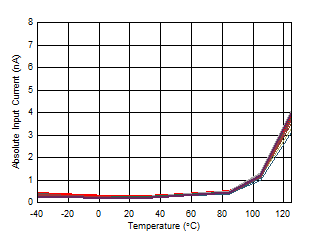
Analog Input Current Absolute Input Current vs Temperature, V(AINX) = 0 V
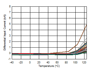
Differential Input Current vs Temperature, VIN = 2.5 V
Figure 7-6
Figure 7-7
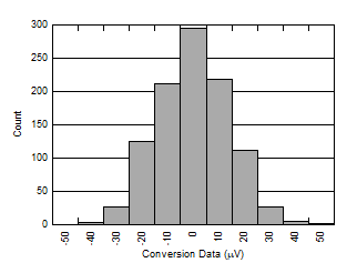
Noise Distribution (Gain = 0.1875, Data Rate = 1.2 kSPS)
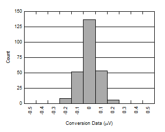
Distribution (Gain = 32, Data Rate = 20 SPS)
Figure 7-8
Figure 7-9
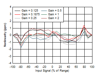
Nonlinearity vs Input Voltage (Gain = 0.125 to 2)
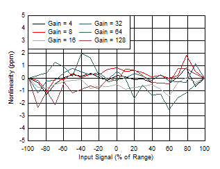
vs Input Voltage (Gain = 4 to 128)
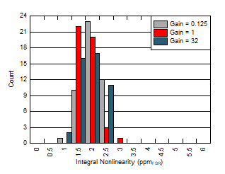
Distribution (Gain = 0.125, 1, 32)
Figure 7-10
Figure 7-11
Figure 7-12
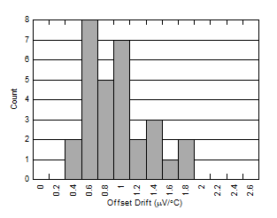
Offset Error Drift Distribution (Gain = 0.125)
Drift Distribution (Gain = 1)
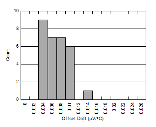
Drift Distribution (Gain = 32)
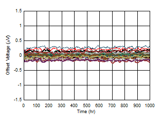
Long-Term Drift (Gain = 0.1875)
Long-Term Drift (Gain = 32)
Figure 7-13
Figure 7-14
Figure 7-15
Figure 7-16
Figure 7-17
Gain Error Distribution (Gain = 0.125, 1, 32)
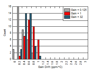
Drift Distribution (Gain = 0.125, 1, 32)
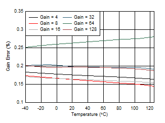
vs Temperature (Gain = 0.125 to 2)
vs Temperature (Gain = 4 to 128)
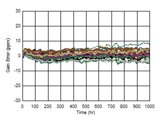
Long-Term Drift (Gain = 0.1875)
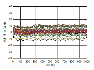
Long-Term Drift (Gain = 32)
Figure 7-18
Figure 7-19
Figure 7-20
Figure 7-21
Figure 7-22
Figure 7-23
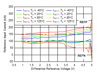
Reference Input Current vs Reference Voltage (TA = -40°C, 25°C, 85°C, 125°C) Figure 7-24
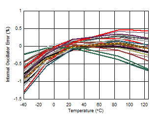
Oscillator Frequency Error vs Temperature
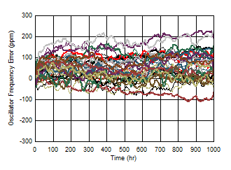
Long-Term Drift
Figure 7-25
Figure 7-26
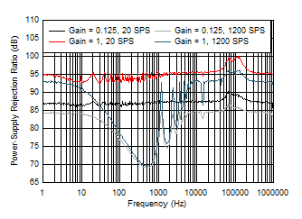
Power-Supply Rejection Ratio (PSRR) vs Frequency (HV_AVDD and HV_AVSS)
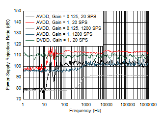
vs Frequency (AVDD and DVDD)
Figure 7-27
Figure 7-28
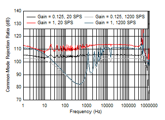
Common-Mode Rejection Ratio (CMRR) vs Frequency Figure 7-29
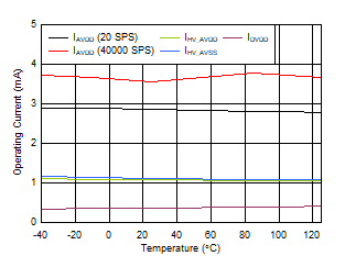
Operating Current vs Temperature Figure 7-30
GUID-D185EE9C-CF88-439A-B5BE-34C1F98E76C7-low.gif
V(AINx) = 0 V
Figure 7-6 Absolute Analog Input Current vs Temperature
GUID-2C8DC5E7-E69B-49CA-9620-6E975E140D32-low.gif
Gain = 0.1875, data rate = 1200 SPS, sinc1 filter, calibrated offset, en = 13.6 µVRMS
Figure 7-8 Conversion Data Distribution
GUID-C8A9A5FE-BCBD-4B5E-BA5A-A536BF39AF7E-low.gif
 
Figure 7-10 Nonlinearity vs Input Signal
GUID-5AA840E8-5DE7-4207-B27F-F2AC9ED01E6C-low.gif
 
Figure 7-12 Nonlinearity Distribution
GUID-B987EC41-876C-4973-9307-9028B10F4C5E-low.gif
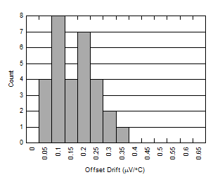
Gain = 1
Figure 7-14 Offset Error Drift Distribution
GUID-8CD8329F-8DAF-4608-9C2E-81FD253D72D0-low.gif
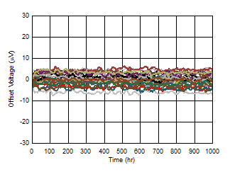
32 units, gain = 0.1875, after calibration
Figure 7-16 Offset Error Long-Term Drift
GUID-EB5D461E-6A2C-441B-AE1D-99A700C3C225-low.gif
 
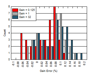
Figure 7-18 Gain Error Distribution
GUID-CC971B63-8A16-4D1A-8D9C-BEBDBD7DCD03-low.gif
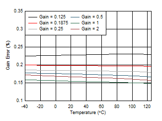
Gain = 0.125 to 2
Figure 7-20 Gain Error vs Temperature
GUID-E44E397B-9514-4D31-BC5B-96B24BA3305C-low.gif
32 units, gain = 0.1875, after calibration
Figure 7-22 Gain Long-Term Drift
GUID-30AAF595-2146-43C2-938D-74683F31832C-low.gif
 
Figure 7-24 Reference Input Current vs Reference Voltage
GUID-7E7BA494-C63A-4781-892B-5725EF46F757-low.gif
32 units, normalized data
Figure 7-26 Oscillator Frequency Long-Term Drift
GUID-357AAF19-BB43-4B13-9708-0B207537F6A8-low.gif
AVDD and DVDD
Figure 7-28 PSRR vs Frequency
GUID-A9FA920E-37B1-4F64-A473-0D54D2852DD9-low.gif
All gains
Figure 7-30 Operating Current vs Temperature
GUID-2DF55A8E-DDF3-45DF-94B5-0AFC4CA37D58-low.gif
VIN = 2.5 V
Figure 7-7 Differential Analog Input Current vs Temperature
GUID-7651DE56-28A9-40A2-A25C-CBCC62579B5D-low.gif
Gain = 32, data rate = 20 SPS, FIR filter, calibrated offset,
en = 0.076 µVRMS
Figure 7-9 Conversion Data Distribution
GUID-7AE94F99-A81A-4B12-A0B6-2A12471A1D3B-low.gif
 
Figure 7-11 Nonlinearity vs Input Signal
GUID-15650A0A-7FA5-487A-95E7-5CBE10B79A45-low.gif
Gain = 0.125
Figure 7-13 Offset Error Drift Distribution
GUID-8377EE16-9E41-482C-B8F7-8AFE67F5A51E-low.gif
Gain = 32
Figure 7-15 Offset Error Drift Distribution
GUID-98C13706-2104-41AF-A847-B24B4A9E4DDD-low.gif
32 units, gain = 32, after calibration
Figure 7-17 Offset Error Long-Term Drift
GUID-EA6FAD29-FF37-48D3-A0F5-32DEAF7C9C7B-low.gif
 
Figure 7-19 Gain Drift Distribution
GUID-1A37C089-C3A8-4B71-A647-61E3707E6ACA-low.gif
Gain = 4 to 128
Figure 7-21 Gain Error vs Temperature
GUID-9AB9E1C3-C47F-4F5C-ABE0-F99E5C013462-low.gif
32 units, gain = 32, after calibration
Figure 7-23 Gain Long-Term Drift
GUID-5279421D-402C-4181-B5D7-38AF63C45E63-low.gif
32 units
Figure 7-25 Oscillator Frequency Error vs Temperature
GUID-0189AA72-D0B9-4513-89AD-E5352DF9C517-low.gif
HV_AVDD and HV_AVSS
Figure 7-27 PSRR vs Frequency
GUID-200982A2-15D0-4FBA-9D73-B41CBC2B66BC-low.gif
 
Figure 7-29 CMRR vs Frequency