ZHCSJI6 March 2019 TPS65653-Q1
PRODUCT PREVIEW Information. Product in design phase of development. Subject to change or discontinuance without notice.
- 1 特性
- 2 应用
- 3 说明
- 4 修订历史记录
- 5 Pin Configuration and Functions
- 6 Specifications
-
7 Detailed Description
- 7.1 Overview
- 7.2 Functional Block Diagram
- 7.3
Feature Description
- 7.3.1 DC/DC Converters
- 7.3.2 Sync Clock Functionality
- 7.3.3 Power-Up
- 7.3.4 Regulator Control
- 7.3.5 Enable and Disable Sequences
- 7.3.6 Device Reset Scenarios
- 7.3.7 Diagnosis and Protection Features
- 7.3.8 Operation of the GPO Signals
- 7.3.9 Digital Signal Filtering
- 7.4 Device Functional Modes
- 7.5 Programming
- 7.6
Register Maps
- 7.6.1
Register Descriptions
- 7.6.1.1 DEV_REV
- 7.6.1.2 OTP_REV
- 7.6.1.3 BUCK0_CTRL_1
- 7.6.1.4 BUCK0_CTRL_2
- 7.6.1.5 BUCK1_CTRL_1
- 7.6.1.6 BUCK1_CTRL_2
- 7.6.1.7 BUCK0_VOUT
- 7.6.1.8 BUCK1_VOUT
- 7.6.1.9 BUCK0_DELAY
- 7.6.1.10 BUCK1_DELAY
- 7.6.1.11 GPO_DELAY
- 7.6.1.12 GPO2_DELAY
- 7.6.1.13 GPO_CTRL
- 7.6.1.14 CONFIG
- 7.6.1.15 PLL_CTRL
- 7.6.1.16 PGOOD_CTRL_1
- 7.6.1.17 PGOOD_CTRL_2
- 7.6.1.18 PG_FAULT
- 7.6.1.19 RESET
- 7.6.1.20 INT_TOP_1
- 7.6.1.21 INT_TOP_2
- 7.6.1.22 INT_BUCK
- 7.6.1.23 TOP_STAT
- 7.6.1.24 BUCK_STAT
- 7.6.1.25 TOP_MASK_1
- 7.6.1.26 TOP_MASK_2
- 7.6.1.27 BUCK_MASK
- 7.6.1.28 SEL_I_LOAD
- 7.6.1.29 I_LOAD_2
- 7.6.1.30 I_LOAD_1
- 7.6.1
Register Descriptions
- 8 Application and Implementation
- 9 Power Supply Recommendations
- 10Layout
- 11器件和文档支持
7.3.5 Enable and Disable Sequences
The TPS65653-Q1 device supports start-up and shutdown sequencing with programmable delays for different regulator outputs using single EN control signal. The Buck regulator is selected for delayed control with:
- BUCKx_EN = 1 in BUCKx_CTRL_1 register
- BUCKx_EN_PIN_CTRL = 1 in BUCKx_CTRL_1 register
- BUCKx_VSET[7:0] bits in BUCKx_VOUT register defines the voltage when EN pin is high
- The delay from rising edge of EN pin to the regulator enable is set by BUCKx_STARTUP_DELAY[3:0] bits in BUCKx_DELAY register and
- The delay from falling edge of EN pin to the regulator disable is set by BUCKx_SHUTDOWN_DELAY[3:0] bits in BUCKx_DELAY register.
The GPO (and GPO2) digital output signals can be also controlled as a part of start-up and shutdown sequencing with the following settings:
- GPOx_EN = 1 in GPO_CTRL register
- GPOx_EN_PIN_CTRL = 1 in GPO_CTRL register
- The delay from rising edge of EN pin to the rising edge of GPO/GPO2 signal is set by GPOx_STARTUP_DELAY[3:0] bits in GPOx_DELAY register and
- The delay from falling edge of EN pin to the falling edge of GPO/GPO2 signal is set by GPOx_SHUTDOWN_DELAY[3:0] bits in GPOx_DELAY register.
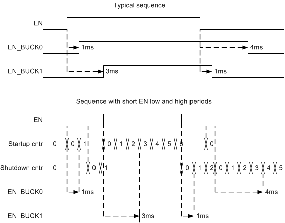
An example of the start-up and shutdown sequences for the buck regulators are shown in Figure 10. The start-up and shutdown delays for the Buck0 regulator are 1 ms and 4 ms; for the Buck1 regulator start-up and shutdown delays are 3 ms and 1 ms. The delay settings are used only for enable/disable control with EN signal.
 Figure 10. Start-Up and Shutdown Sequencing