ZHCSDT4D June 2015 – September 2020 BQ29209-Q1
PRODUCTION DATA
- 1 特性
- 2 应用
- 3 说明
- 4 Revision History
- 5 Device Options
- 6 Pin Configuration and Functions
- 7 Specifications
- 8 Detailed Description
- 9 Application and Implementation
- 10Power Supply Recommendations
- 11Layout
- 12Device and Documentation Support
- 13Mechanical, Packaging, and Orderable Information
封装选项
请参考 PDF 数据表获取器件具体的封装图。
机械数据 (封装 | 引脚)
- DRB|8
散热焊盘机械数据 (封装 | 引脚)
- DRB|8
订购信息
8.3.7 Customer Test Mode
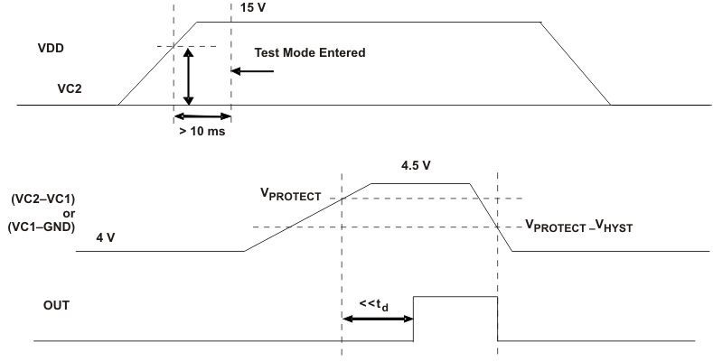
Customer Test Mode (CTM) helps to greatly reduce the overvoltage detection delay time and enable quicker customer production testing. This mode is intended for quick-pass board-level verification tests, and, as such, individual cell overvoltage levels may deviate slightly from the specifications (VPROTECT, VOA). If accurate overvoltage thresholds are to be tested, use the standard delay settings that are intended for normal use.
To enter CTM, VDD should be set to approximately 9.5 V higher than VC2. When CTM is entered, the device switches from the normal overvoltage delay time scale factor, XDELAY, to a significantly reduced factor of approximately 0.08, thereby reducing the delay time during an overvoltage condition.
Avoid exceeding any Absolute Maximum Voltages on any pins when placing the part into CTM. Also, avoid exceeding absolute maximum voltages for the individual cell voltages (VC1–GND) and (VC2–VC1). Stressing the pins beyond the rated limits may cause permanent damage to the device.
To exit CTM, power off the device and then power it back on.
 Figure 8-4 Voltage Test Limits