ZHCSDT4D June   2015  – September 2020 BQ29209-Q1

PRODUCTION DATA  

  1. 特性
  2. 应用
  3. 说明
  4. Revision History
  5. Device Options
  6. Pin Configuration and Functions
    1.     Pin Functions
  7. Specifications
    1. 7.1 Absolute Maximum Ratings
    2. 7.2 ESD Ratings
    3. 7.3 Recommended Operating Conditions
    4. 7.4 Thermal Information
    5. 7.5 Electrical Characteristics
    6. 7.6 Recommended Cell Balancing Configurations
    7. 7.7 Typical Characteristics
  8. Detailed Description
    1. 8.1 Overview
      1. 8.1.1 Voltage Protection
      2. 8.1.2 Cell Balancing
    2. 8.2 Functional Block Diagram
    3. 8.3 Feature Description
      1. 8.3.1 Protection (OUT) Timing
      2. 8.3.2 Cell Voltage > VPROTECT
      3. 8.3.3 Cell Connection Sequence
      4. 8.3.4 Cell Balance Enable Control
      5. 8.3.5 Cell Balance Configuration
      6. 8.3.6 Cell Imbalance Auto-Detection (Via Cell Voltage)
      7. 8.3.7 Customer Test Mode
      8. 8.3.8 Test Conditions
    4. 8.4 Device Functional Modes
      1. 8.4.1 NORMAL Mode
      2. 8.4.2 PROTECTION Mode
  9. Application and Implementation
    1. 9.1 Application Information
    2. 9.2 Typical Applications
      1. 9.2.1 Battery Connection
        1. 9.2.1.1 Design Requirements
        2. 9.2.1.2 Detailed Design Procedure
        3. 9.2.1.3 Application Curve
    3. 9.3 System Example
      1. 9.3.1 External Cell Balancing
  10. 10Power Supply Recommendations
  11. 11Layout
    1. 11.1 Layout Guidelines
    2. 11.2 Layout Example
  12. 12Device and Documentation Support
    1. 12.1 Documentation Support
    2. 12.2 接收文档更新通知
    3. 12.3 支持资源
    4. 12.4 Trademarks
    5. 12.5 静电放电警告
    6. 12.6 术语表
  13. 13Mechanical, Packaging, and Orderable Information

封装选项

请参考 PDF 数据表获取器件具体的封装图。

机械数据 (封装 | 引脚)
  • DRB|8
散热焊盘机械数据 (封装 | 引脚)
订购信息

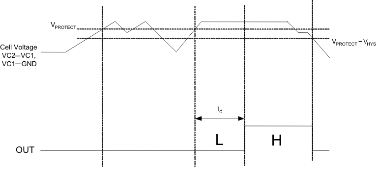
Cell Voltage > VPROTECT

When one or both of the cell voltages rises above VPROTECT, the internal comparator is tripped, and the delay begins to count to td. If the input remains above VPROTECT for the duration of td, the BQ29209-Q1 output changes from a low to a high state, by means of an internal pull-up network, to a regulated voltage of no more than 9.5 V when IOH = 0 mA.

The external delay capacitor should charge up to no more than the internal LDO voltage (approximately 5 V typically), and will fully discharge in approximately under 100 ms when the overvoltage condition is removed.
GUID-634D3B4D-303A-4225-880B-CD931429E502-low.gifFigure 8-1 Timing for Overvoltage Sensing