TIDUEW7 May 2020
- Description
- Resources
- Features
- Applications
- Design Images
- 1System Description
-
2System Overview
- 2.1 Block Diagram
- 2.2 Design Considerations
- 2.3 Highlighted Products
- 2.4 System Design Theory
- 3Getting Started, Testing Setup, and Test Results
- 4Design Files
- 5Software Files
- 6Related Documentation
3.1.1 Hardware
This section contains information about the initial set-up of the TIDA-050043 board, power-up options and user interfaces. Figure 23 shows the top side of the fully assembled PCB with labels to help locate connectors or switches on the boards.
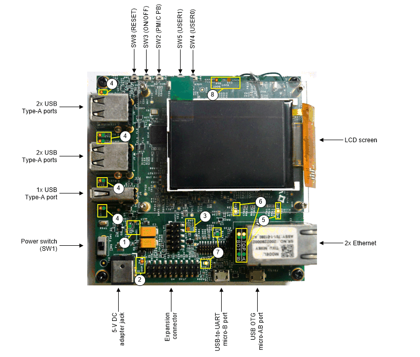
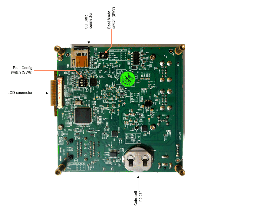
Figure 24 shows the bottom side of the fully assembled PCB with labels.
The following is a list of steps that must be followed to set up the hardware of the system.
- Attach stand-offs to the board with screws inserted in the four holes at the edge of the PCB.
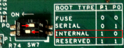
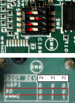
- Set the BOOT option using SW7/SW6 DIP switches (Figure 25 and Figure 26).
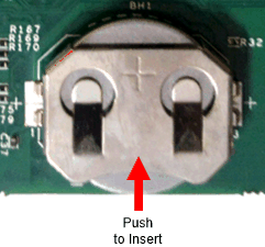
- Insert CR2032 coin-cell battery in the holder BH1 (Figure 27).
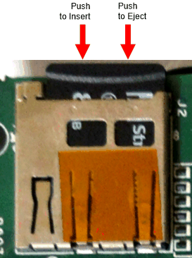
- Insert the SD card in J2 connector, if SD Card is used for BOOT (Figure 28).
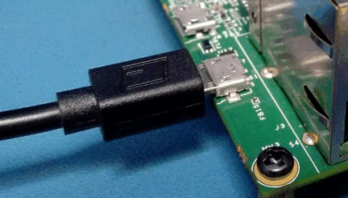
- Insert the USB micro-B cable into J8 connector for UART debug in Terminal window (Figure 29). Type-A plug connects to computer USB port
- Insert the 5-V DC adapter barrel jack into J1 connector to supply power (Figure 30). SMI24-5-V-P6 from CUI Inc is the recommended power supply.
- Set SW1 to the ON position.
- After BOOT is complete, connect the desired peripherals. For example: RJ-45 Ethernet (J3), LCD screen (J9), USB device (J4, J5, J6, J7).
NOTE
The voltage of the coin-cell battery (3.0 V nominal) must be above 2.4 V for the supervisor to allow system power-on. If the coin-cell battery voltage is too low, it must be replaced with a fresh battery to continue testing.
NOTE
Refer to Section 3.1.2 for the procedure to debug TIDA-050043 through Terminal window

NOTE
Power supplies other than the SMI24-5-V-P6 may be substituted if the DC output voltage, current rating, polarity, and barrel jack size (inside diameter and outside diameter) are equivalent. Power supplies with DC voltage greater than 5.25V are not acceptable because of the over voltage protection circuit on the board which is intended to prevent damage to the ICs.
NOTE
It is always recommended to power-down the system by switching SW1 to the OFF position before unplugging the DC adapter power supply.