TIDUEW7 May 2020
- Description
- Resources
- Features
- Applications
- Design Images
- 1System Description
-
2System Overview
- 2.1 Block Diagram
- 2.2 Design Considerations
- 2.3 Highlighted Products
- 2.4 System Design Theory
- 3Getting Started, Testing Setup, and Test Results
- 4Design Files
- 5Software Files
- 6Related Documentation
2.4.5 BOOT Configuration
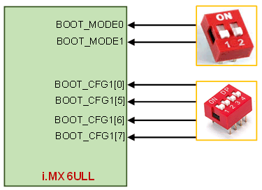
This design uses two sets of BOOT configuration switches. BOOT Mode pins are controlled by SW7 DIP switches that are connected to dedicated BOOT_MODE0 and BOOT_MODE1 input pins of i.MX 6ULL Processor. Along with these, there are 24 different pins for setting Boot Config which shares pins with LCD Data. Of these 24 pins, 4 of them are controlled by the 4 DIP Switches of SW6. All of the possible BOOT options for this design are given in Table 5 (SW7) and Table 6 (SW6). The connections of the DIP switches to the processor are shown in Figure 20
Figure 20. BOOT Mode and Configuration DIP Switches 

Table 5. SW7 BOOT Mode Settings
| SW7, PIN 1 | SW7, PIN 2 | |
|---|---|---|
| BOOT Type | BOOT_MODE[1] | BOOT_MODE[0] |
| Boot from Fuses | 0 | 0 |
| Serial Download | 0 | 1 |
| Internal BOOT | 1 | 0 |
| Reserved | 1 | 1 |
Table 6. SW6 BOOT Config Settings
| SW6, PIN 4 | SW6, PIN 3 | SW6, PIN 2 | SW2, PIN 1 | |
|---|---|---|---|---|
| BOOT Device | BOOT_CFG1[7] | BOOT_CFG1[6] | BOOT_CFG1[5] | BOOT_CFG1[0](2) |
| QSPI | 0 | 0 | 0 | x |
| SD, eSD, SDXC | 0 | 1 | 0 | x |
| eMMC(1) | 0 | 1 | 1 | x |
(1) To select boot device as eMMC, an assembly change must also be performed. See schematic for details.
(2) BT_CFG1[0] is used for SD loopback clock selection.