SPRUJ51 june   2023


  1.   1
  2. 1Abstract
  3. 2EVM Revisions and Assembly Variants
    1. 2.1 Inside the Box
    2. 2.2 EMC, EMI and ESD Compliance
  4.   Trademarks
  5. 3System Description
    1. 3.1 Key Features
      1. 3.1.1 Processor
      2. 3.1.2 Power Supply
      3. 3.1.3 Memory
      4. 3.1.4 JTAG Emulator
      5. 3.1.5 Supported Interfaces and Peripherals
      6. 3.1.6 Expansion Connectors Headers to Support Application Specific Add On Boards
    2. 3.2 Functional Block Diagram
    3. 3.3 AM62x-Low Power SK EVM Interface Mapping
    4. 3.4 Power ON OFF Procedures
      1. 3.4.1 Power-On Procedure
      2. 3.4.2 Power-Off Procedure
      3. 3.4.3 Power Test Points
    5. 3.5 Peripheral and Major Component Description
      1. 3.5.1  Clocking
      2. 3.5.2  Reset
      3. 3.5.3  OLDI Display Interface
      4. 3.5.4  CSI Interface
      5. 3.5.5  Audio Codec Interface
      6. 3.5.6  HDMI Display Interface
      7. 3.5.7  JTAG Interface
      8. 3.5.8  Test Automation Header
      9. 3.5.9  UART Interface
      10. 3.5.10 USB Interface
        1. 3.5.10.1 USB 2.0 Type A Interface
        2. 3.5.10.2 USB 2.0 Type C Interface
      11. 3.5.11 Memory Interfaces
        1. 3.5.11.1 LPDDR4 Interface
        2. 3.5.11.2 OSPI Interface
        3. 3.5.11.3 MMC Interfaces
          1. 3.5.11.3.1 MMC0 - eMMC Interface
          2. 3.5.11.3.2 MMC1 - Micro SD Interface
          3. 3.5.11.3.3 MMC2 - M2 Key E Interface
        4. 3.5.11.4 EEPROM
      12. 3.5.12 Ethernet Interface
        1. 3.5.12.1 CPSW Ethernet PHY1 Default Configuration
        2. 3.5.12.2 CPSW Ethernet PHY2 Default Configuration
      13. 3.5.13 GPIO Port Expander
      14. 3.5.14 GPIO Mapping
      15. 3.5.15 Power
        1. 3.5.15.1 Power Requirements
        2. 3.5.15.2 Power Input
        3. 3.5.15.3 Power Supply
        4. 3.5.15.4 Power Sequencing
        5. 3.5.15.5 AM62x 17x17 SoC Power
        6. 3.5.15.6 Current Monitoring
      16. 3.5.16 AM62x-Low Power SK EVM User Setup and Configuration
        1. 3.5.16.1 EVM DIP Switches
        2. 3.5.16.2 Boot Modes
        3. 3.5.16.3 User Test LEDs
      17. 3.5.17 Expansion Headers
        1. 3.5.17.1 User Expansion Connector
        2. 3.5.17.2 MCU Connector
        3. 3.5.17.3 PRU Connector
      18. 3.5.18 Push Buttons
      19. 3.5.19 I2C Address Mapping
  6. 4Known Issues and Modifications
  7. 5Revision History
  8. 6IMPORTANT NOTICE AND DISCLAIMER

JTAG Interface

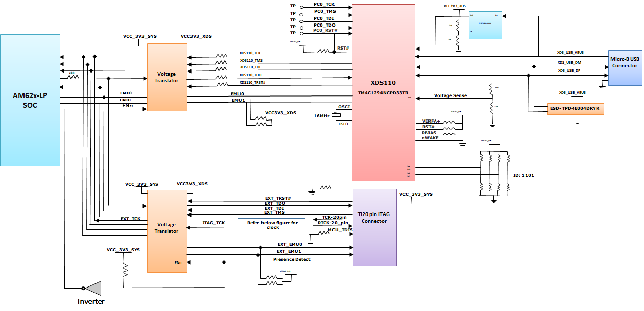
The AM62x Low-Power SK EVM board includes XDS110 class on board emulation. The connection for the emulator uses an USB 2.0 micro-B connector and the circuit acts as a Bus powered USB device. The VBUS power from the connector will be used to power the emulation circuit such that connection to the emulator is not lost when the power to the SKEVM is removed. Voltage translation buffers are used to isolate the XDS110 circuit from the rest of the SKEVM. Optionally, JTAG Interface on SKEVM is also provided through 20 Pin Standard JTAG cTI Header J19. This allows the user to connect an external JTAG Emulator Cable. Voltage translation buffers are used to isolate the JTAG signals from cTI header from the rest of the SKEVM. The output from the voltage translators from XDS110 Section and cTI Header Section are muxed and connected to AM62X JTAG Interface. If a connection to the cTI 20 Pin JTAG connector is sensed using a presence detect circuit, the mux will be set to route the 20 pin signals from the cTI connector to the AM62X SoC in place of the on-board emulation circuit.
GUID-20230519-SS0I-HWQB-K0VQ-TXRGGNQBHKRT-low.png Figure 3-13 JTAG Interface Block Diagram

The pin-out of the cTI 20 pin JTAG connector are given in Table 3-6. A ESD protection part number TPD4E004 is provided on USB signals to steer ESD current pulses to VCC or GND. TPD4E004 protects against ESD pulses up to ±15-kV Human-Body Model (HBM) as specified in IEC 61000-4-2 and provides ±8-kV contact discharge and ±12- kV air-gap discharge.

Table 3-6 JTAG Connector (J19) Pinout
Pin No. Signal
1 JTAG_TMS
2 JTAG_TRST#
3 JTAG_TDI
4 JTAG_TDIS
5 VCC3V3_SYS
6 NC
7 JTAG_TDO
8 SEL_XDS110_INV
9 JTAG_cTI_RTCK
10 DGND
11 JTAG_cTI_TCK
12 DGND
13 JTAG_EMU0
14 JTAG_EMU1
15 JTAG_EMU_RSTn
16 DGND
17 NC
18 NC
19 NC
20 DGND

The pin-outs of the cTI 20 pin JTAG connector are given in the table above. A ESD protection part number TPD4E004 is provided on USB signals to steer ESD current pulses to VCC or GND. TPD4E004 protects against ESD pulses up to ±15-kV Human-Body Model (HBM) as specified in IEC 61000-4-2 and provides ±8-kV contact discharge and ±12- kV air-gap discharge.