SPRUJ51 june 2023
- 1
- 1Abstract
- 2EVM Revisions and Assembly Variants
- Trademarks
-
3System Description
- 3.1 Key Features
- 3.2 Functional Block Diagram
- 3.3 AM62x-Low Power SK EVM Interface Mapping
- 3.4 Power ON OFF Procedures
- 3.5
Peripheral and Major Component Description
- 3.5.1 Clocking
- 3.5.2 Reset
- 3.5.3 OLDI Display Interface
- 3.5.4 CSI Interface
- 3.5.5 Audio Codec Interface
- 3.5.6 HDMI Display Interface
- 3.5.7 JTAG Interface
- 3.5.8 Test Automation Header
- 3.5.9 UART Interface
- 3.5.10 USB Interface
- 3.5.11 Memory Interfaces
- 3.5.12 Ethernet Interface
- 3.5.13 GPIO Port Expander
- 3.5.14 GPIO Mapping
- 3.5.15 Power
- 3.5.16 AM62x-Low Power SK EVM User Setup and Configuration
- 3.5.17 Expansion Headers
- 3.5.18 Push Buttons
- 3.5.19 I2C Address Mapping
- 4Known Issues and Modifications
- 5Revision History
- 6IMPORTANT NOTICE AND DISCLAIMER
3.5.11.2 OSPI Interface
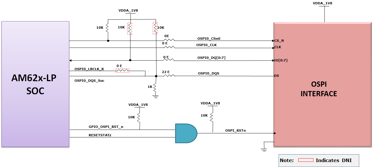
The AM62x Low-Power SK EVM board has a 1-Gbit OSPI memory device from Cypress Part# W35N01JWTBAG which is connected to the OSPI0 interface of the AM62x 17x17 SoC. The OSPI interface supports single and double data rates with clock speeds up to 166Mhz STR and 120Mhz DTR.
OSPI & QSPI implementation: 0 ohm resistors are provided for DATA[7:0], DQS, INT# and CLK signals. Footprints to mount external pull up resistors are provided on DATA[7:0] to prevent bus floating. The footprint for the OSPI memory also allows the installation of either a QSPI memory or an OSPI memory. The 0 ohm series resistors provided for pins OSPI_DATA[4:7] will be removed if QSPI flash is to be mounted.
The reset for the OSPI flash is connected to a circuit that ANDs the RESETSTATz from the SoC with the signal GPIO_OSPI_RSTn from the SoC GPIO. This will apply reset for warm and cold reset. A pull-up is provided on GPIO_OSPI_RSTn coming from SoC pin to set the default active state.
The OSPI flash is powered by 1.8V IO supply. The 1.8V supply is provided to both VCC and VCCQ pins of the OSPI flash memory. The OSPI interface of the SOC is powered by VDDSHV1 Power group of SoC and is connected to 1.8V IO supply.
 Figure 3-19 OSPI Interface block Diagram