ZHCSOY9 december 2021 UCC28781
PRODUCTION DATA
- 1
- 1 特性
- 2 应用
- 3 说明
- 4 Revision History
- 5 Pin Configuration and Functions
- 6 Specifications
-
7 Detailed Description
- 7.1 Overview
- 7.2 Functional Block Diagram
- 7.3
Detailed Pin Description
- 7.3.1 BUR Pin (Programmable Burst Mode)
- 7.3.2 FB Pin (Feedback Pin)
- 7.3.3 REF Pin (Internal 5-V Bias)
- 7.3.4 VDD Pin (Device Bias Supply)
- 7.3.5 P13 and SWS Pins
- 7.3.6 S13 Pin
- 7.3.7 IPC Pin (Intelligent Power Control Pin)
- 7.3.8 RUN Pin (Driver and Bias Source for Isolator)
- 7.3.9 PWMH and AGND Pins
- 7.3.10 PWML and PGND Pins
- 7.3.11 SET Pin
- 7.3.12 RTZ Pin (Sets Delay for Transition Time to Zero)
- 7.3.13 RDM Pin (Sets Synthesized Demagnetization Time for ZVS Tuning)
- 7.3.14 XCD Pin
- 7.3.15 CS, VS, and FLT Pins
- 7.4
Device Functional Modes
- 7.4.1 Adaptive ZVS Control with Auto-Tuning
- 7.4.2 Dead-Time Optimization
- 7.4.3 EMI Dither and Dither Fading Function
- 7.4.4 Control Law Across Entire Load Range
- 7.4.5 Adaptive Amplitude Modulation (AAM)
- 7.4.6 Adaptive Burst Mode (ABM)
- 7.4.7 Low Power Mode (LPM)
- 7.4.8 First Standby Power Mode (SBP1)
- 7.4.9 Second Standby Power Mode (SBP2)
- 7.4.10 Startup Sequence
- 7.4.11 Survival Mode of VDD (INT_STOP)
- 7.4.12
System Fault Protections
- 7.4.12.1 Brown-In and Brown-Out
- 7.4.12.2 Output Over-Voltage Protection (OVP)
- 7.4.12.3 输入过压保护 (IOVP)
- 7.4.12.4 FLT 引脚上的过热保护 (OTP)
- 7.4.12.5 CS 引脚上的过热保护 (OTP)
- 7.4.12.6 可编程过功率保护 (OPP)
- 7.4.12.7 峰值功率限制 (PPL)
- 7.4.12.8 输出短路保护 (SCP)
- 7.4.12.9 过流保护 (OCP)
- 7.4.12.10 External Shutdown
- 7.4.12.11 Internal Thermal Shutdown
- 7.4.13 Pin Open/Short Protections
-
8 Application and Implementation
- 8.1 Application Information
- 8.2
Typical Application Circuit
- 8.2.1 Design Requirements for a 60-W, 15-V ZVSF Bias Supply Application with a DC Input
- 8.2.2 Detailed Design Procedure
- 8.2.3 Application Curves
- 9 Power Supply Recommendations
- 10Layout
- 11Device and Documentation Support
- 12Mechanical, Packaging, and Orderable Information
7.4.12.6 可编程过功率保护 (OPP)
过功率保护 (OPP) 允许在有限的时间内和过功率条件下运行,因此 UCC28781 能够支持具有临时峰值功率要求的功率级设计。如下图所示(IVSL 上的 VCST OPP 曲线),当 VCST 高于 OPP 曲线的阈值电压 (VCST(OPP)) 时,将启动 160ms 计时器。如果 VCST 持续高于 VCST(OPP) 长达 160ms,则 1.5s 计时器启动,控制器保持故障状态而无需切换。较长的恢复时间可降低持续过功率事件期间的平均电流。系统优势包括降低高密度适配器中的热应力以及保护其输出电缆。
OPP 功能使用 IVSL 作为线路前馈信号,根据 VBULK 来改变 VCST(OPP),以便使 OPP 触发点在宽线路电压范围内保持恒定。UCC28781 能够通过 CS 引脚和电流检测电阻器 (RCS) 之间连接的电阻器 (ROPP) 在 CS 引脚上添加线路补偿失调电压,从而实现 OPP 曲线的可编程性。从 CS 引脚流出的内部电流源会在 ROPP 上产生失调电压。该电流电平等于 IVSL 除以 KLC 的恒定增益。随着 ROPP 的增加,OPP 触发点在高压线路上变得更低,因此允许较低的峰值磁化电流持续运行。
OPP 功能使用 VVS 作为输出电压前馈信号,将依赖于线路的 VCST(OPP) 曲线修改为两个不同的集,从而使 OPP 触发点在宽输出电压范围内更加一致。VVS 高于 2.5V 时的较高 OPP 阈值包含两个分段线性区域,而 VVS 低于 2.4V 时的较低 OPP 阈值包含一个分段线性区域。
OPP 曲线的最高阈值 (VCST(OPP1)) 为 0.6V,有助于确定 VBULK(MIN) 时的 RCS 值。
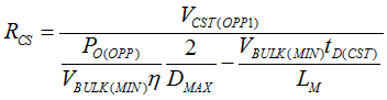
- 其中 PO(OPP) 是触发 OPP 的输出功率
- tD(CST) 是峰值电流环路中所有延迟的总和,会导致额外的峰值电流过冲
tD(CST) 包括低侧驱动器的传播延迟、电流检测滤波器延迟 (ROPP x CCS)、内部 CS 比较器延迟 (tD(CS)) 和 QL 的非线性电容延迟。确定 RCS 后,可以调整 ROPP,在最高线保持类似的 OPP 点。请注意,如果所设置 OPP 触发点与全功率差距过大,可能会给散热设计带来更多挑战,因为只要相应的峰值电流略小于 OPP 阈值,转换器就会以更大的功率持续运行。
 图 7-43 IVSL 上的 VCST OPP 曲线
 图 7-44 OPP 时序图