ZHCSOY9 december 2021 UCC28781
PRODUCTION DATA
- 1
- 1 特性
- 2 应用
- 3 说明
- 4 Revision History
- 5 Pin Configuration and Functions
- 6 Specifications
-
7 Detailed Description
- 7.1 Overview
- 7.2 Functional Block Diagram
- 7.3
Detailed Pin Description
- 7.3.1 BUR Pin (Programmable Burst Mode)
- 7.3.2 FB Pin (Feedback Pin)
- 7.3.3 REF Pin (Internal 5-V Bias)
- 7.3.4 VDD Pin (Device Bias Supply)
- 7.3.5 P13 and SWS Pins
- 7.3.6 S13 Pin
- 7.3.7 IPC Pin (Intelligent Power Control Pin)
- 7.3.8 RUN Pin (Driver and Bias Source for Isolator)
- 7.3.9 PWMH and AGND Pins
- 7.3.10 PWML and PGND Pins
- 7.3.11 SET Pin
- 7.3.12 RTZ Pin (Sets Delay for Transition Time to Zero)
- 7.3.13 RDM Pin (Sets Synthesized Demagnetization Time for ZVS Tuning)
- 7.3.14 XCD Pin
- 7.3.15 CS, VS, and FLT Pins
- 7.4
Device Functional Modes
- 7.4.1 Adaptive ZVS Control with Auto-Tuning
- 7.4.2 Dead-Time Optimization
- 7.4.3 EMI Dither and Dither Fading Function
- 7.4.4 Control Law Across Entire Load Range
- 7.4.5 Adaptive Amplitude Modulation (AAM)
- 7.4.6 Adaptive Burst Mode (ABM)
- 7.4.7 Low Power Mode (LPM)
- 7.4.8 First Standby Power Mode (SBP1)
- 7.4.9 Second Standby Power Mode (SBP2)
- 7.4.10 Startup Sequence
- 7.4.11 Survival Mode of VDD (INT_STOP)
- 7.4.12
System Fault Protections
- 7.4.12.1 Brown-In and Brown-Out
- 7.4.12.2 Output Over-Voltage Protection (OVP)
- 7.4.12.3 输入过压保护 (IOVP)
- 7.4.12.4 FLT 引脚上的过热保护 (OTP)
- 7.4.12.5 CS 引脚上的过热保护 (OTP)
- 7.4.12.6 可编程过功率保护 (OPP)
- 7.4.12.7 峰值功率限制 (PPL)
- 7.4.12.8 输出短路保护 (SCP)
- 7.4.12.9 过流保护 (OCP)
- 7.4.12.10 External Shutdown
- 7.4.12.11 Internal Thermal Shutdown
- 7.4.13 Pin Open/Short Protections
-
8 Application and Implementation
- 8.1 Application Information
- 8.2
Typical Application Circuit
- 8.2.1 Design Requirements for a 60-W, 15-V ZVSF Bias Supply Application with a DC Input
- 8.2.2 Detailed Design Procedure
- 8.2.3 Application Curves
- 9 Power Supply Recommendations
- 10Layout
- 11Device and Documentation Support
- 12Mechanical, Packaging, and Orderable Information
7.4.1 Adaptive ZVS Control with Auto-Tuning
Figure 7-21 shows the simplified block diagram explaining the ZVS control of the UCC28781 controller. A high-voltage sensing network provides a replica of the switch node voltage waveform (VSW) with a limited “visible” lower voltage range that the SWS pin can handle. The ZVS discriminator identifies the ZVS condition and determines the adjustment direction for the on-time of PWMH (tDM) by detecting if VSW reaches a predetermined ZVS threshold, VTH(SWS), within tZ, where tZ is the targeted zero voltage transition time of VSW controlled by the PWMH-to-PWML dead-time optimizer.
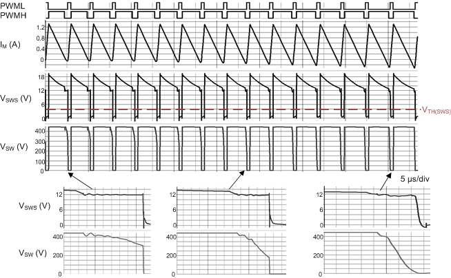
In Figure 7-21, VSW of the current switching cycle in the dashed line has not reached VTH(SWS) after tZ expires. The ZVS discriminator sends a TUNE signal to increase tDM for the next switching cycle in the solid line, such that the negative magnetizing current (IM-) can be increased to bring VSW down to a lower level in the same tZ. After a few switching cycles, the tDM optimizer settles and locks into ZVS operation of the low-side switch (QL). In steady-state, there is a fine adjustment on tDM, which is the least significant bit (LSB) of the ZVS tuning loop. This small change of tDM in each switching cycle is too small to significantly move the ZVS condition away from the desired operating point. Figure 7-22 demonstrates how fast the ZVS control can lock into ZVS operation. Before the ZVS loop is settled, controller starts in a valley-switching mode as tDM is not long enough to create sufficient IM-. Within 15 switching cycles, the ZVS tuning loop settles and begins toggling tDM with an LSB.
 Figure 7-21 Block Diagram of Adaptive ZVS
Control
 Figure 7-22 Auto-Tuning Process of
Adaptive ZVS Control