ZHCSOY9 december 2021 UCC28781
PRODUCTION DATA
- 1
- 1 特性
- 2 应用
- 3 说明
- 4 Revision History
- 5 Pin Configuration and Functions
- 6 Specifications
-
7 Detailed Description
- 7.1 Overview
- 7.2 Functional Block Diagram
- 7.3
Detailed Pin Description
- 7.3.1 BUR Pin (Programmable Burst Mode)
- 7.3.2 FB Pin (Feedback Pin)
- 7.3.3 REF Pin (Internal 5-V Bias)
- 7.3.4 VDD Pin (Device Bias Supply)
- 7.3.5 P13 and SWS Pins
- 7.3.6 S13 Pin
- 7.3.7 IPC Pin (Intelligent Power Control Pin)
- 7.3.8 RUN Pin (Driver and Bias Source for Isolator)
- 7.3.9 PWMH and AGND Pins
- 7.3.10 PWML and PGND Pins
- 7.3.11 SET Pin
- 7.3.12 RTZ Pin (Sets Delay for Transition Time to Zero)
- 7.3.13 RDM Pin (Sets Synthesized Demagnetization Time for ZVS Tuning)
- 7.3.14 XCD Pin
- 7.3.15 CS, VS, and FLT Pins
- 7.4
Device Functional Modes
- 7.4.1 Adaptive ZVS Control with Auto-Tuning
- 7.4.2 Dead-Time Optimization
- 7.4.3 EMI Dither and Dither Fading Function
- 7.4.4 Control Law Across Entire Load Range
- 7.4.5 Adaptive Amplitude Modulation (AAM)
- 7.4.6 Adaptive Burst Mode (ABM)
- 7.4.7 Low Power Mode (LPM)
- 7.4.8 First Standby Power Mode (SBP1)
- 7.4.9 Second Standby Power Mode (SBP2)
- 7.4.10 Startup Sequence
- 7.4.11 Survival Mode of VDD (INT_STOP)
- 7.4.12
System Fault Protections
- 7.4.12.1 Brown-In and Brown-Out
- 7.4.12.2 Output Over-Voltage Protection (OVP)
- 7.4.12.3 输入过压保护 (IOVP)
- 7.4.12.4 FLT 引脚上的过热保护 (OTP)
- 7.4.12.5 CS 引脚上的过热保护 (OTP)
- 7.4.12.6 可编程过功率保护 (OPP)
- 7.4.12.7 峰值功率限制 (PPL)
- 7.4.12.8 输出短路保护 (SCP)
- 7.4.12.9 过流保护 (OCP)
- 7.4.12.10 External Shutdown
- 7.4.12.11 Internal Thermal Shutdown
- 7.4.13 Pin Open/Short Protections
-
8 Application and Implementation
- 8.1 Application Information
- 8.2
Typical Application Circuit
- 8.2.1 Design Requirements for a 60-W, 15-V ZVSF Bias Supply Application with a DC Input
- 8.2.2 Detailed Design Procedure
- 8.2.3 Application Curves
- 9 Power Supply Recommendations
- 10Layout
- 11Device and Documentation Support
- 12Mechanical, Packaging, and Orderable Information
8.2.2.2.3 Primary Winding Turns (NP)
The number of turns on the primary winding (NP) of the transformer is determined by two design considerations:
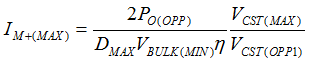
- The maximum flux density (BMAX) must be kept below the saturation limit (BSAT) of the chosen magnetic core under the highest peak magnetizing current (IM+(MAX)) condition, the cross-sectional area (AE) of the core, and highest core temperature. When IFB = 0 A, such as during VO soft-start or step-up load transient, the peak magnetizing current reaches IM+(MAX), since VCST = VCST(MAX) in those conditions. IM+(MAX) can be estimated based on the output power triggering an OPP fault (PO(OPP)) with VCST = VCST(OPP1) at VBULK(MIN). Equation 25.
 Equation 26.
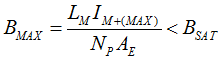
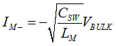
- The AC flux density (ΔB) affects the core loss of the transformer. For a transition-mode ZVS flyback, the core loss is usually highest at high line, since the switching frequency is highest, duty cycle is smallest, and peak-to-peak magnetizing current swing is greatest for a given load condition. The following equation is the ΔB calculation including the contribution of negative magnetizing current (IM-), used to put into the Steinmetz equation for more accurate core loss estimation. For VBULK ≥ NPS(VO+VF), IM- is calculated with VBULK divided by the characteristic impedance of LM and the lumped time-related switch-node capacitance (CSW). IM- is always a negative value. The expression of fSW is derived based on the triangular approximation of the magnetizing current, which also considers the effect of IM- over wide DC or AC input line conditions. Equation 27.
 Equation 28.
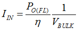 Equation 29.
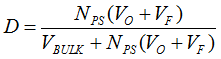 Equation 30.
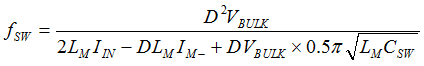 Equation 31.
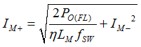 Equation 32.
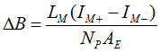
For the ΔB calculation, remember that IM- is a negative value and that ΔB is a peak-to-peak flux swing. Core loss is based on ½ of ΔB.