ZHCSOY9 december 2021 UCC28781
PRODUCTION DATA
- 1
- 1 特性
- 2 应用
- 3 说明
- 4 Revision History
- 5 Pin Configuration and Functions
- 6 Specifications
-
7 Detailed Description
- 7.1 Overview
- 7.2 Functional Block Diagram
- 7.3
Detailed Pin Description
- 7.3.1 BUR Pin (Programmable Burst Mode)
- 7.3.2 FB Pin (Feedback Pin)
- 7.3.3 REF Pin (Internal 5-V Bias)
- 7.3.4 VDD Pin (Device Bias Supply)
- 7.3.5 P13 and SWS Pins
- 7.3.6 S13 Pin
- 7.3.7 IPC Pin (Intelligent Power Control Pin)
- 7.3.8 RUN Pin (Driver and Bias Source for Isolator)
- 7.3.9 PWMH and AGND Pins
- 7.3.10 PWML and PGND Pins
- 7.3.11 SET Pin
- 7.3.12 RTZ Pin (Sets Delay for Transition Time to Zero)
- 7.3.13 RDM Pin (Sets Synthesized Demagnetization Time for ZVS Tuning)
- 7.3.14 XCD Pin
- 7.3.15 CS, VS, and FLT Pins
- 7.4
Device Functional Modes
- 7.4.1 Adaptive ZVS Control with Auto-Tuning
- 7.4.2 Dead-Time Optimization
- 7.4.3 EMI Dither and Dither Fading Function
- 7.4.4 Control Law Across Entire Load Range
- 7.4.5 Adaptive Amplitude Modulation (AAM)
- 7.4.6 Adaptive Burst Mode (ABM)
- 7.4.7 Low Power Mode (LPM)
- 7.4.8 First Standby Power Mode (SBP1)
- 7.4.9 Second Standby Power Mode (SBP2)
- 7.4.10 Startup Sequence
- 7.4.11 Survival Mode of VDD (INT_STOP)
- 7.4.12
System Fault Protections
- 7.4.12.1 Brown-In and Brown-Out
- 7.4.12.2 Output Over-Voltage Protection (OVP)
- 7.4.12.3 输入过压保护 (IOVP)
- 7.4.12.4 FLT 引脚上的过热保护 (OTP)
- 7.4.12.5 CS 引脚上的过热保护 (OTP)
- 7.4.12.6 可编程过功率保护 (OPP)
- 7.4.12.7 峰值功率限制 (PPL)
- 7.4.12.8 输出短路保护 (SCP)
- 7.4.12.9 过流保护 (OCP)
- 7.4.12.10 External Shutdown
- 7.4.12.11 Internal Thermal Shutdown
- 7.4.13 Pin Open/Short Protections
-
8 Application and Implementation
- 8.1 Application Information
- 8.2
Typical Application Circuit
- 8.2.1 Design Requirements for a 60-W, 15-V ZVSF Bias Supply Application with a DC Input
- 8.2.2 Detailed Design Procedure
- 8.2.3 Application Curves
- 9 Power Supply Recommendations
- 10Layout
- 11Device and Documentation Support
- 12Mechanical, Packaging, and Orderable Information
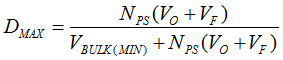
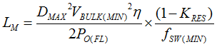
8.2.2.2.2 Primary Magnetizing Inductance (LM)
After NPS is chosen, LM can be estimated based on minimum switching frequency (fSW(MIN)) at VBULK(MIN), maximum duty cycle (DMAX), and output power at highest nominal output voltage, nominal full-load current (PO(FL)). The choice of fSW(MIN) should consider the expected range of switching frequency as bulk voltage increases from minimum to maximum and as load falls from maximum to the burst mode threshold. KRES represents the duty cycle loss to wait for the switch-node voltage transition from the reflected output voltage to zero. Typically, fSW may extend to 200% to 300% fSW(MIN) or higher. A KRES value of 5% to 6% is used as an initial estimate for GaN-based power stages, while ~10% is more appropriate for Si-based designs. The selection of minimum switching frequency (fSW(MIN)) should consider the impact on full-load efficiency and EMI filter design.