ZHCSOY9 december 2021 UCC28781
PRODUCTION DATA
- 1
- 1 特性
- 2 应用
- 3 说明
- 4 Revision History
- 5 Pin Configuration and Functions
- 6 Specifications
-
7 Detailed Description
- 7.1 Overview
- 7.2 Functional Block Diagram
- 7.3
Detailed Pin Description
- 7.3.1 BUR Pin (Programmable Burst Mode)
- 7.3.2 FB Pin (Feedback Pin)
- 7.3.3 REF Pin (Internal 5-V Bias)
- 7.3.4 VDD Pin (Device Bias Supply)
- 7.3.5 P13 and SWS Pins
- 7.3.6 S13 Pin
- 7.3.7 IPC Pin (Intelligent Power Control Pin)
- 7.3.8 RUN Pin (Driver and Bias Source for Isolator)
- 7.3.9 PWMH and AGND Pins
- 7.3.10 PWML and PGND Pins
- 7.3.11 SET Pin
- 7.3.12 RTZ Pin (Sets Delay for Transition Time to Zero)
- 7.3.13 RDM Pin (Sets Synthesized Demagnetization Time for ZVS Tuning)
- 7.3.14 XCD Pin
- 7.3.15 CS, VS, and FLT Pins
- 7.4
Device Functional Modes
- 7.4.1 Adaptive ZVS Control with Auto-Tuning
- 7.4.2 Dead-Time Optimization
- 7.4.3 EMI Dither and Dither Fading Function
- 7.4.4 Control Law Across Entire Load Range
- 7.4.5 Adaptive Amplitude Modulation (AAM)
- 7.4.6 Adaptive Burst Mode (ABM)
- 7.4.7 Low Power Mode (LPM)
- 7.4.8 First Standby Power Mode (SBP1)
- 7.4.9 Second Standby Power Mode (SBP2)
- 7.4.10 Startup Sequence
- 7.4.11 Survival Mode of VDD (INT_STOP)
- 7.4.12
System Fault Protections
- 7.4.12.1 Brown-In and Brown-Out
- 7.4.12.2 Output Over-Voltage Protection (OVP)
- 7.4.12.3 输入过压保护 (IOVP)
- 7.4.12.4 FLT 引脚上的过热保护 (OTP)
- 7.4.12.5 CS 引脚上的过热保护 (OTP)
- 7.4.12.6 可编程过功率保护 (OPP)
- 7.4.12.7 峰值功率限制 (PPL)
- 7.4.12.8 输出短路保护 (SCP)
- 7.4.12.9 过流保护 (OCP)
- 7.4.12.10 External Shutdown
- 7.4.12.11 Internal Thermal Shutdown
- 7.4.13 Pin Open/Short Protections
-
8 Application and Implementation
- 8.1 Application Information
- 8.2
Typical Application Circuit
- 8.2.1 Design Requirements for a 60-W, 15-V ZVSF Bias Supply Application with a DC Input
- 8.2.2 Detailed Design Procedure
- 8.2.3 Application Curves
- 9 Power Supply Recommendations
- 10Layout
- 11Device and Documentation Support
- 12Mechanical, Packaging, and Orderable Information
8.2.2.1 Input Bulk Capacitance and Minimum Bulk Voltage
For off-line rectified-AC applications, the total input bulk capacitor (CBULK) should be sized to provide energy from the peak of the minimum input AC-line rms voltage (VIN(MIN)) to the minimum allowable voltage (VBULK(MIN)) for the power conversion stage. Due to the transition-mode operation, too low of VBULK(MIN) selection results in higher rms current at VIN(MIN) and affects the full-load efficiency, while too high of VBULK(MIN) enlarges the volume of the bulk capacitor. This equation does not account for the hold-up time requirement over AC-line dips and drop-outs.
Equation 19. 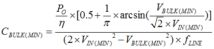
For DC-input applications, the value of CBULK depends on the nature of the input:
- If the DC source is subject to brief
interruptions (similar to dips and drop-outs of an AC-line), then the value of
CBULK is calculated in a similar manner as for
CBULK(MIN) above. ΔtDC_drop represents the maximum
expected interruption time of the DC input.Equation 20.
- If the DC source is consistently steady such as from a high-voltage battery, then the value of CBULK should be sufficient to effectively by-pass the high-frequency primary switching current to avoid conducting significant EMI noise back to the source.CBULK may be made up of more than one capacitor. Select standard values with sufficient margin to the calculated CBULK(MIN) to allow for tolerance and aging.