ZHCSL07C September 2019 – August 2021 TPS8802
PRODUCTION DATA
- 1 特性
- 2 应用
- 3 说明
- 4 Revision History
- 5 Pin Configuration and Functions
- 6 Specifications
- 7 Typical Characteristics
-
8 Detailed Description
- 8.1 Overview
- 8.2 Functional Block Diagram
- 8.3
Feature Description
- 8.3.1 System Power-up
- 8.3.2 LDO Regulators
- 8.3.3 Photo Chamber AFE
- 8.3.4 LED Driver
- 8.3.5 Carbon Monoxide Sensor AFE
- 8.3.6 Boost Converter
- 8.3.7 Interconnect Driver
- 8.3.8 Piezoelectric Horn Driver
- 8.3.9 Battery Test
- 8.3.10 AMUX
- 8.3.11 Analog Bias Block and 8 MHz Oscillator
- 8.3.12 Interrupt Signal Alerts
- 8.4 Device Functional Modes
- 8.5 Programming
- 8.6
Register Maps
- 8.6.1 REVID Register (Offset = 0h) [reset = 0h]
- 8.6.2 STATUS1 Register (Offset = 1h) [reset = 0h]
- 8.6.3 STATUS2 Register (Offset = 2h) [reset = 0h]
- 8.6.4 MASK Register (Offset = 3h) [reset = 0h]
- 8.6.5 CONFIG1 Register (Offset = 4h) [reset = 20h]
- 8.6.6 CONFIG2 Register (Offset = 5h) [reset = 2h]
- 8.6.7 ENABLE1 Register (Offset = 6h) [reset = 10h]
- 8.6.8 ENABLE2 Register (Offset = 7h) [reset = 0h]
- 8.6.9 CONTROL Register (Offset = 8h) [reset = 0h]
- 8.6.10 SLPTMR1 Register (Offset = 9h) [reset = 0h]
- 8.6.11 SLPTMR2 Register (Offset = Ah) [reset = 0h]
- 8.6.12 GPIO_AMUX Register (Offset = Bh) [reset = 0h]
- 8.6.13 CO_BATTEST Register (Offset = Ch) [reset = 0h]
- 8.6.14 CO Register (Offset = Dh) [reset = 0h]
- 8.6.15 VBOOST Register (Offset = Eh) [reset = F2h]
- 8.6.16 LEDLDO Register (Offset = Fh) [reset = 0h]
- 8.6.17 PH_CTRL Register (Offset = 10h) [reset = 0h]
- 8.6.18 LED_DAC_A Register (Offset = 11h) [reset = 0h]
- 8.6.19 LED_DAC_B Register (Offset = 12h) [reset = 0h]
- 9 Application and Implementation
- 10Power Supply Recommendations
- 11Layout
- 12Device and Documentation Support
- 13Mechanical, Packaging, and Orderable Information
8.3.6 Boost Converter
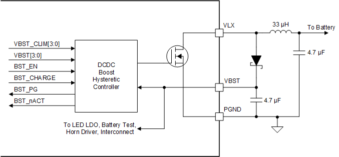
 Figure 8-7 DC to DC Hysteretic Boost
Circuit
Figure 8-7 DC to DC Hysteretic Boost
CircuitThe boost converter operates with a wide range of input and output voltages to support multiple battery configurations and driver voltages. The boost converter output VBST is internally connected to the LED LDO, interconnect driver, horn driver, and battery test load, and may be externally connected to VCC. The boost converter has a power-good register bit BST_PG to notify the MCU when the boost converter is above 95% of the target voltage. The BST_PG signal is deglitched for 200 μs to prevent load transients from causing a false indication. If the BST_PG signal is low after 10 ms of enabling the boost or changing the VBST setting, the BST_ERR signal latches high. The BST_PG signal reads low if the boost converter is disabled.
The boost converter is enabled if any of the following conditions are met:
- BST_EN = 1 or BST_CHARGE=1, except if SLP_BST = 1 and SLP_EN = 1
- VCCLOW_BST = 1 and the deglitched VCCLOW comparator trips
- Device is in MCULDO_ERR state
The SLP_BST signal disables the boost while the device is in sleep mode if the boost is enabled with BST_EN. The BST_CHARGE register bit enables the boost converter until the BST_PG signal is high, at which point BST_CHARGE resets to 0 and the boost converter is disabled. VCCLOW_BST enables the boost if the deglitched VCCLOW comparator trips. MCULDO_ERR state also enables the boost converter.
A specific I2C command sequence must be used when enabling the boost converter and disabling the photo amplifier. Do not enable the boost converter (changing BST_EN from 0 to 1) and disable the photo input amplifier (changing PAMP_EN from 1 to 0) in the same I2C command. Use either of the following I2C command sequences to enable the boost converter and disable the photo input amplifier:
- Write BST_EN=1 and PAMP_EN=1, then write BST_EN=1 and PAMP_EN=0
- Write BST_EN=0 and PAMP_EN=0, then write BST_EN=1 and PAMP_EN=0