ZHCSL07C September 2019 – August 2021 TPS8802
PRODUCTION DATA
- 1 特性
- 2 应用
- 3 说明
- 4 Revision History
- 5 Pin Configuration and Functions
- 6 Specifications
- 7 Typical Characteristics
-
8 Detailed Description
- 8.1 Overview
- 8.2 Functional Block Diagram
- 8.3
Feature Description
- 8.3.1 System Power-up
- 8.3.2 LDO Regulators
- 8.3.3 Photo Chamber AFE
- 8.3.4 LED Driver
- 8.3.5 Carbon Monoxide Sensor AFE
- 8.3.6 Boost Converter
- 8.3.7 Interconnect Driver
- 8.3.8 Piezoelectric Horn Driver
- 8.3.9 Battery Test
- 8.3.10 AMUX
- 8.3.11 Analog Bias Block and 8 MHz Oscillator
- 8.3.12 Interrupt Signal Alerts
- 8.4 Device Functional Modes
- 8.5 Programming
- 8.6
Register Maps
- 8.6.1 REVID Register (Offset = 0h) [reset = 0h]
- 8.6.2 STATUS1 Register (Offset = 1h) [reset = 0h]
- 8.6.3 STATUS2 Register (Offset = 2h) [reset = 0h]
- 8.6.4 MASK Register (Offset = 3h) [reset = 0h]
- 8.6.5 CONFIG1 Register (Offset = 4h) [reset = 20h]
- 8.6.6 CONFIG2 Register (Offset = 5h) [reset = 2h]
- 8.6.7 ENABLE1 Register (Offset = 6h) [reset = 10h]
- 8.6.8 ENABLE2 Register (Offset = 7h) [reset = 0h]
- 8.6.9 CONTROL Register (Offset = 8h) [reset = 0h]
- 8.6.10 SLPTMR1 Register (Offset = 9h) [reset = 0h]
- 8.6.11 SLPTMR2 Register (Offset = Ah) [reset = 0h]
- 8.6.12 GPIO_AMUX Register (Offset = Bh) [reset = 0h]
- 8.6.13 CO_BATTEST Register (Offset = Ch) [reset = 0h]
- 8.6.14 CO Register (Offset = Dh) [reset = 0h]
- 8.6.15 VBOOST Register (Offset = Eh) [reset = F2h]
- 8.6.16 LEDLDO Register (Offset = Fh) [reset = 0h]
- 8.6.17 PH_CTRL Register (Offset = 10h) [reset = 0h]
- 8.6.18 LED_DAC_A Register (Offset = 11h) [reset = 0h]
- 8.6.19 LED_DAC_B Register (Offset = 12h) [reset = 0h]
- 9 Application and Implementation
- 10Power Supply Recommendations
- 11Layout
- 12Device and Documentation Support
- 13Mechanical, Packaging, and Orderable Information
8.4.1 Sleep Mode
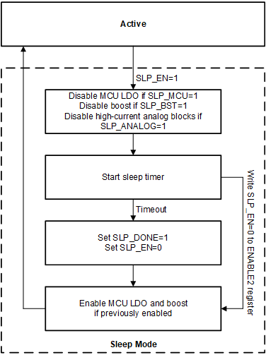
 Figure 8-13 Sleep Mode State Diagram
The device integrates a sleep timer to manage critical analog and regulator blocks independent of the external microcontroller. When sleep mode is enabled, the timer starts and various blocks (MCU LDO, boost, or drivers and amplifiers) are disabled depending on the CONFIG1 register configuration. After the sleep timer finishes, SLP_EN is reset and the SLP_DONE bit in STATUS1 register is latched high and can be configured to output through the GPIO or INT_MCU pins. This notifies the microcontroller that the sleep timer is finished and sleep mode is exited. Alternatively, sleep mode is exited by writing zero to the SLP_EN bit. Writing zero to SLP_EN does not trigger the SLP_DONE bit in the STATUS1 register. Figure 8-14 shows the sleep mode state diagram.
Sleep mode reduces power consumption in three ways:
- by quickly disabling analog blocks
- by powering off the boost and MCU LDO during sleep mode
- by allowing the MCU to enter its lowest power idle state
Every I2C transaction takes time and consumes a small amount of power. The SLP_ANALOG bit configures sleep mode to disable high-power amplifiers and drivers simultaneously when entering sleep mode. This functionality can save several I2C transactions and reduces time that the amplifiers and drivers are idly enabled.
The device may require the boost converter and MCU LDO while the microcontroller is performing sensing and testing operations, but may not require the boost and MCU LDO while the microcontroller is in its idle state. SLP_BST and SLP_MCU disable the boost converter and MCU LDO during sleep mode. If the boost converter and MCU LDO were previously enabled, they are re-enabled when sleep mode is exited. This process reduces system current consumption caused by the MCU LDO and boost converter while preventing a system brown-out if the MCU loses power, because the exit of sleep mode returns power to the MCU.
During sleep mode operation, the MCU can enter its lowest power idle state and monitor a GPIO pin for the SLP_DONE interrupt signal. This monitoring allows the MCU clocks to be disabled as the sleep timer signals the MCU to wake up after a precise programmed time. The amount of time is programmable from 1 ms to 65535 ms in 1 ms intervals in the SLPTMR1 and SLPTMR2 registers.
The device is nearly fully functional in sleep mode. The microcontroller can access all registers and configure all blocks. Only three functions are disabled in sleep mode:
- boost converter inactivity timer
- the MCULDO fault state
- over-temperature shutdown fault state
The MCULDO undervoltage and system over-temperature monitors remain enabled if the MCU LDO and OTS monitors are enabled, so as soon as the device exits sleep mode, the system enters the fault state that corresponds to any detected fault.