ZHCSK61B August 2019 – December 2019 TPS66120 , TPS66121
PRODUCTION DATA.
- 1 特性
- 2 应用
- 3 说明
- 4 修订历史记录
- 5 Pin Configuration and Functions
-
6 Specifications
- 6.1 Absolute Maximum Ratings
- 6.2 ESD Ratings
- 6.3 Recommended Operating Conditions
- 6.4 Recommended Supply Load Capacitance
- 6.5 Thermal Information
- 6.6 PPHV Power Switch Characteristics
- 6.7 Power Path Supervisory
- 6.8 VBUS LDO Characteristics
- 6.9 Thermal Shutdown Characteristics
- 6.10 Input-output (I/O) Characteristics
- 6.11 Power Consumption Characteristics
- 6.12 Typical Characteristics
- 7 Detailed Description
- 8 Application and Implementation
- 9 Power Supply Recommendations
- 10Layout
- 11器件和文档支持
- 12机械、封装和可订购信息
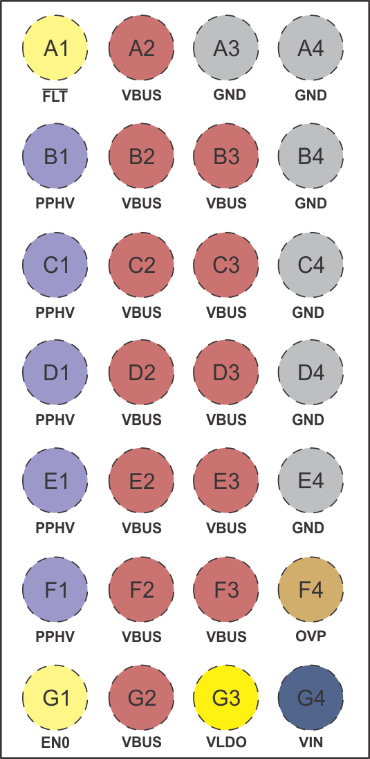
5 Pin Configuration and Functions
TPS6612x YBG Package
28-Pin WCSP
Top View

Pin Functions
| Pin | I/O | Reset State | Description | |
|---|---|---|---|---|
| Name | No. | |||
| PPHV | B1, C1, D1, E1, F1 | Power | Off | HV System Supply from VBUS. Bypass with capacitance CPPHV to GND. |
| VBUS | A2, B2, B3, C2, C3, D2, D3, E2, E3, F2, F3, G2 | Power | - | 4V to 20V nominal input supply to PPHV. Bypass with capacitance CVBUS to GND. |
| VIN | G4 | Power | - | Device input supply. Bypass with capacitance CVIN to GND. |
| VLDO | G3 | Power | - | VIN supply or VBUS LDO regulated supply output from power multipexer. Bypass with capacitance CVLDO to GND. |
| GND | A3, A4, B4, C4, D4, E4 | Ground | - | Ground. Connect all pins to ground plane. |
| OVP | F4 | Analog | - | Selects VBUS OVP. Tie pin to VBUS resistor divider output to set desired VBUS OVP level. Tie pin to GND to remove VBUS OVP function. |
| EN0 | G1 | Digital Input | Pull-down | Enable PPHV sink path. Internal pull-down. |
| FLT | A1 | Digital OUtput | Hi-Z | Fault Output Indicator. Active low. This pin is a true open-drain (no PMOS). Float pin when unused. |