ZHCSK61B August 2019 – December 2019 TPS66120 , TPS66121
PRODUCTION DATA.
- 1 特性
- 2 应用
- 3 说明
- 4 修订历史记录
- 5 Pin Configuration and Functions
-
6 Specifications
- 6.1 Absolute Maximum Ratings
- 6.2 ESD Ratings
- 6.3 Recommended Operating Conditions
- 6.4 Recommended Supply Load Capacitance
- 6.5 Thermal Information
- 6.6 PPHV Power Switch Characteristics
- 6.7 Power Path Supervisory
- 6.8 VBUS LDO Characteristics
- 6.9 Thermal Shutdown Characteristics
- 6.10 Input-output (I/O) Characteristics
- 6.11 Power Consumption Characteristics
- 6.12 Typical Characteristics
- 7 Detailed Description
- 8 Application and Implementation
- 9 Power Supply Recommendations
- 10Layout
- 11器件和文档支持
- 12机械、封装和可订购信息
7.3.4.1 Supply Connections
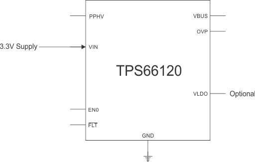
Figure 9 shows the TPS66120 VIN being supplied from a 3.3-V supply. The VLDO output may or may not be used to supply other circuitry in the application, for example a PD Controller. During dead battery, the internal 3.3-V VBUS LDO provides power to the TPS66120 and the VLDO output. Once VIN input supply becomes available, the VBUS LDO is disabled and VIN provides power to the VLDO output.
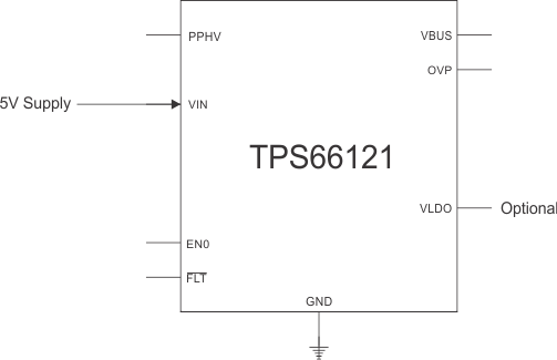
Figure 10 shows the TPS66121 VIN being supplied from a 5-V supply. The VLDO output may or may not be used to supply power to external circuitry. During dead battery, the internal 5-V VBUS LDO provides power to the TPS66121 and the VLDO output. Once VIN input supply becomes available, the VBUS LDO is disabled and VIN provides power to the VLDO output.
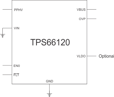
Another option is to power the TPS66120 from the VBUS LDO only as shown in Figure 11. Since VIN is tied to GND, power to the TPS66120 is provided by the 3.3-V VBUS LDO when VBUS power is present. The VLDO output may be used optionally to supply power to external circuitry.
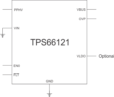
Similarly, Figure 12 shows the TPS66121 being powered from the VBUS LDO only. Since VIN is tied to GND, power to the TPS66121 is provided by the 5-V VBUS LDO when VBUS power is present. The VLDO output may be used optionally to supply power to external circuitry.
 Figure 9. TPS66120 VIN 3.3-V Supply
  Figure 10. TPS66121 VIN 5-V Supply
  Figure 11. TPS66120 VBUS Powered
  Figure 12. TPS66121 VBUS Powered