ZHCSK61B August   2019  – December  2019 TPS66120 , TPS66121

PRODUCTION DATA.  

  1. 特性
  2. 应用
  3. 说明
    1.     功能表
      1.      TPS6612x 方框图
  4. 修订历史记录
  5. Pin Configuration and Functions
    1.     Pin Functions
  6. Specifications
    1. 6.1  Absolute Maximum Ratings
    2. 6.2  ESD Ratings
    3. 6.3  Recommended Operating Conditions
    4. 6.4  Recommended Supply Load Capacitance
    5. 6.5  Thermal Information
    6. 6.6  PPHV Power Switch Characteristics
    7. 6.7  Power Path Supervisory
    8. 6.8  VBUS LDO Characteristics
    9. 6.9  Thermal Shutdown Characteristics
    10. 6.10 Input-output (I/O) Characteristics
    11. 6.11 Power Consumption Characteristics
    12. 6.12 Typical Characteristics
  7. Detailed Description
    1. 7.1 Overview
    2. 7.2 Functional Block Diagram
    3. 7.3 Feature Description
      1. 7.3.1 20-V Sink (PPHV Power Path)
        1. 7.3.1.1 PPHV Soft Start
        2. 7.3.1.2 PPHV Reverse Current Protection (RCP)
      2. 7.3.2 Overtemperature Protection
      3. 7.3.3 VBUS Overvoltage Protection (OVP)
      4. 7.3.4 Power Management and Supervisory
        1. 7.3.4.1 Supply Connections
        2. 7.3.4.2 Power Up Sequences
          1. 7.3.4.2.1 Normal Power Up
          2. 7.3.4.2.2 Dead Battery Operation
    4. 7.4 Device Functional Modes
      1. 7.4.1 State Transitions
        1. 7.4.1.1 DISABLED State
        2. 7.4.1.2 SNK State
      2. 7.4.2 SNK FAULT State
      3. 7.4.3 Device Functional Mode Summary
      4. 7.4.4 Enabling the PPHV Sink Path
      5. 7.4.5 Faults
        1. 7.4.5.1 Fault Types
  8. Application and Implementation
    1. 8.1 Application Information
    2. 8.2 Typical Application
      1. 8.2.1 Design Requirements
      2. 8.2.2 Detailed Design Procedure
        1. 8.2.2.1 External VLDO Capacitor (CVLDO)
        2. 8.2.2.2 PPHV, VBUS Power Path Capacitance
        3. 8.2.2.3 VBUS TVS Protection (Optional)
        4. 8.2.2.4 VBUS Schottky Diode Protection (Optional)
        5. 8.2.2.5 VBUS Overvoltage Protection (Optional)
        6. 8.2.2.6 Dead Battery Support
      3. 8.2.3 Application Curves
  9. Power Supply Recommendations
  10. 10Layout
    1. 10.1 Layout Guidelines
    2. 10.2 Layout Example
  11. 11器件和文档支持
    1. 11.1 相关链接
    2. 11.2 接收文档更新通知
    3. 11.3 支持资源
    4. 11.4 商标
    5. 11.5 静电放电警告
    6. 11.6 Glossary
  12. 12机械、封装和可订购信息

封装选项

机械数据 (封装 | 引脚)
散热焊盘机械数据 (封装 | 引脚)

Typical Application

Figure 17 shows a USB Type-C single port design using a power delivery controller. For this system, a single 5-V supply in the system is used to supply power to the external load switch, as well as, the connector VCONN power. The VIN terminal of the TPS66121 is tied to GND and the TPS66121 is powered by the VBUS LDO once VBUS is present. In addition, the TPS66121 supplies power to the 5-V supply of the PD controller via the VLDO output. The PPHV integrated power path provides power to the system and battery charger from VBUS when the TPS66121 Sink path is enabled. An external 5-V load switch is shown to provide power to VBUS when system is configured as a Source.
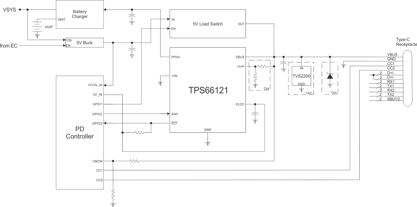
TPS66120 TPS66121 fig_app_sink_sp_bus_powered.gifFigure 17. Single Port Type-C PD Port Using a 5-V Supply.