ZHCSK61B August   2019  – December  2019 TPS66120 , TPS66121

PRODUCTION DATA.  

  1. 特性
  2. 应用
  3. 说明
    1.     功能表
      1.      TPS6612x 方框图
  4. 修订历史记录
  5. Pin Configuration and Functions
    1.     Pin Functions
  6. Specifications
    1. 6.1  Absolute Maximum Ratings
    2. 6.2  ESD Ratings
    3. 6.3  Recommended Operating Conditions
    4. 6.4  Recommended Supply Load Capacitance
    5. 6.5  Thermal Information
    6. 6.6  PPHV Power Switch Characteristics
    7. 6.7  Power Path Supervisory
    8. 6.8  VBUS LDO Characteristics
    9. 6.9  Thermal Shutdown Characteristics
    10. 6.10 Input-output (I/O) Characteristics
    11. 6.11 Power Consumption Characteristics
    12. 6.12 Typical Characteristics
  7. Detailed Description
    1. 7.1 Overview
    2. 7.2 Functional Block Diagram
    3. 7.3 Feature Description
      1. 7.3.1 20-V Sink (PPHV Power Path)
        1. 7.3.1.1 PPHV Soft Start
        2. 7.3.1.2 PPHV Reverse Current Protection (RCP)
      2. 7.3.2 Overtemperature Protection
      3. 7.3.3 VBUS Overvoltage Protection (OVP)
      4. 7.3.4 Power Management and Supervisory
        1. 7.3.4.1 Supply Connections
        2. 7.3.4.2 Power Up Sequences
          1. 7.3.4.2.1 Normal Power Up
          2. 7.3.4.2.2 Dead Battery Operation
    4. 7.4 Device Functional Modes
      1. 7.4.1 State Transitions
        1. 7.4.1.1 DISABLED State
        2. 7.4.1.2 SNK State
      2. 7.4.2 SNK FAULT State
      3. 7.4.3 Device Functional Mode Summary
      4. 7.4.4 Enabling the PPHV Sink Path
      5. 7.4.5 Faults
        1. 7.4.5.1 Fault Types
  8. Application and Implementation
    1. 8.1 Application Information
    2. 8.2 Typical Application
      1. 8.2.1 Design Requirements
      2. 8.2.2 Detailed Design Procedure
        1. 8.2.2.1 External VLDO Capacitor (CVLDO)
        2. 8.2.2.2 PPHV, VBUS Power Path Capacitance
        3. 8.2.2.3 VBUS TVS Protection (Optional)
        4. 8.2.2.4 VBUS Schottky Diode Protection (Optional)
        5. 8.2.2.5 VBUS Overvoltage Protection (Optional)
        6. 8.2.2.6 Dead Battery Support
      3. 8.2.3 Application Curves
  9. Power Supply Recommendations
  10. 10Layout
    1. 10.1 Layout Guidelines
    2. 10.2 Layout Example
  11. 11器件和文档支持
    1. 11.1 相关链接
    2. 11.2 接收文档更新通知
    3. 11.3 支持资源
    4. 11.4 商标
    5. 11.5 静电放电警告
    6. 11.6 Glossary
  12. 12机械、封装和可订购信息

封装选项

机械数据 (封装 | 引脚)
散热焊盘机械数据 (封装 | 引脚)

Power Management and Supervisory

The TPS6612x Power Management block receives power from VIN or VBUS and generates voltages to provide power to the TPS6612x internal circuitry, as well as, provides power to VLDO. The power supply management and supervisory block is shown in Figure 8.
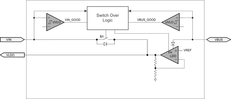
TPS66120 TPS66121 fig_power_supply.gifFigure 8. Power Management and Supervisory

The VLDO terminal may be powered from either VIN or VBUS. The normal power supply input is VIN. When VIN is present, S1 is closed and current flows from VIN to VLDO and the VBUS LDO is disabled. When VIN power is unavailable, as in a dead battery condition, the VBUS LDO will be automatically enabled when VBUS is present, and the VLDO terminal is powered by the VBUS LDO. The Switch Over Logic provides the decision making capability to choose VIN or VBUS power, depending on the state of these voltages (based on their respective UVLO comparators) and their relative levels to each other.