ZHCS089G February   2011  – September 2017 TPS65185

PRODUCTION DATA.  

  1. 特性
  2. 应用
  3. 说明
    1.     Device Images
      1.      典型应用原理图
  4. 修订历史记录
  5. 说明 (续)
  6. Pin Configuration and Functions
    1.     Pin Functions
  7. Specifications
    1. 7.1 Absolute Maximum Ratings
    2. 7.2 ESD Ratings
    3. 7.3 Recommended Operating Conditions
    4. 7.4 Thermal Information
    5. 7.5 Electrical Characteristics
    6. 7.6 Timing Requirements: Data Transmission
    7. 7.7 Typical Characteristics
  8. Detailed Description
    1. 8.1 Overview
    2. 8.2 Functional Block Diagram
    3. 8.3 Feature Description
      1. 8.3.1  Wake-Up and Power-Up Sequencing
      2. 8.3.2  Dependencies Between Rails
      3. 8.3.3  Soft Start
      4. 8.3.4  Active Discharge
      5. 8.3.5  VPOS/VNEG Supply Tracking
      6. 8.3.6  V3P3 Power Switch
      7. 8.3.7  VCOM Adjustment
        1. 8.3.7.1 Kick-Back Voltage Measurement
        2. 8.3.7.2 Storing the VCOM Power-Up Default Value in Memory
      8. 8.3.8  Fault Handling And Recovery
      9. 8.3.9  Power Good Pin
      10. 8.3.10 Interrupt Pin
      11. 8.3.11 Panel Temperature Monitoring
        1. 8.3.11.1 NTC Bias Circuit
        2. 8.3.11.2 Hot, Cold, and Temperature-Change Interrupts
        3. 8.3.11.3 Typical Application of the Temperature Monitor
    4. 8.4 Device Functional Modes
      1. 8.4.1 SLEEP
      2. 8.4.2 STANDBY
      3. 8.4.3 ACTIVE
      4. 8.4.4 Mode Transitions
        1. 8.4.4.1 SLEEP → ACTIVE
        2. 8.4.4.2 SLEEP → STANDBY
        3. 8.4.4.3 STANDBY → ACTIVE
        4. 8.4.4.4 ACTIVE → STANDBY
        5. 8.4.4.5 STANDBY → SLEEP
        6. 8.4.4.6 ACTIVE → SLEEP
    5. 8.5 Programming
      1. 8.5.1 I2C Bus Operation
    6. 8.6 Register Maps
      1. 8.6.1  Thermistor Readout (TMST_VALUE) Register (address = 0x00h) [reset = N/A]
        1. Table 3. TMST_VALUE Register Field Descriptions
      2. 8.6.2  Enable (ENABLE) Register (address = 0x01h) [reset = 0h]
        1. Table 4. ENABLE Register Field Descriptions
      3. 8.6.3  Voltage Adjustment (VADJ) Register (address = 0x02h) [reset = 23h]
        1. Table 5. VADJ Register Field Descriptions
      4. 8.6.4  VCOM 1 (VCOM1) Register (address = 0x03h) [reset = 7Dh]
        1. Table 6. VCOM1 Register Field Descriptions
      5. 8.6.5  VCOM 2 (VCOM2) Register (address = 0x04h) [reset = 04h]
        1. Table 7. VCOM2 Register Field Descriptions
      6. 8.6.6  Interrupt Enable 1 (INT_EN1) Register (address = 0x05h) [reset = 7Fh]
        1. Table 8. INT_EN1 Register Field Descriptions
      7. 8.6.7  Interrupt Enable 2 (INT_EN2) Register (address = 0x06h) [reset = FFh]
        1. Table 9. INT_EN2 Register Field Descriptions
      8. 8.6.8  Interrupt 1 (INT1) Register (address = 0x07h) [reset = 0h]
        1. Table 10. INT1 Register Field Descriptions
      9. 8.6.9  Interrupt 2 (INT2) Register (address = 0x08h) [reset = N/A]
        1. Table 11. INT2 Register Field Descriptions
      10. 8.6.10 Power-Up Sequence 0 (UPSEQ0) Register (address = 0x09h) [reset = E4h]
        1. Table 12. UPSEQ0 Register Field Descriptions
      11. 8.6.11 Power-Up Sequence 1 (UPSEQ1) Register (address = 0x0Ah) [reset = 55h]
        1. Table 13. UPSEQ1 Register Field Descriptions
      12. 8.6.12 Power-Down Sequence 0 (DWNSEQ0) Register (address = 0x0Bh) [reset = 1Eh]
        1. Table 14. DWNSEQ0 Register Field Descriptions
      13. 8.6.13 Power-Down Sequence 1 (DWNSEQ1) Register (address = 0x0Ch) [reset = E0h]
        1. Table 15. DWNSEQ1 Register Field Descriptions
      14. 8.6.14 Thermistor 1 (TMST1) Register (address = 0x0Dh) [reset = 20h]
        1. Table 16. TMST1 Register Field Descriptions
      15. 8.6.15 Thermistor 2 (TMST2) Register (address = 0x0Eh) [reset = 78h]
        1. Table 17. TMST2 Register Field Descriptions
      16. 8.6.16 Power Good Status (PG) Register (address = 0x0Fh) [reset = 0h]
        1. Table 18. PG Register Field Descriptions
      17. 8.6.17 Revision and Version Control (REVID) Register (address = 0x10h) [reset = 45h]
        1. Table 19. REVID Register Field Descriptions
  9. Application and Implementation
    1. 9.1 Application Information
    2. 9.2 Typical Application
      1. 9.2.1 Design Requirements
      2. 9.2.2 Detailed Design Procedure
      3. 9.2.3 Application Curves
  10. 10Power Supply Recommendations
  11. 11Layout
    1. 11.1 Layout Guidelines
    2. 11.2 Layout Example
  12. 12器件和文档支持
    1. 12.1 器件支持
      1. 12.1.1 第三方产品免责声明
    2. 12.2 文档支持
      1. 12.2.1 相关文档
    3. 12.3 接收文档更新通知
    4. 12.4 社区资源
    5. 12.5 商标
    6. 12.6 静电放电警告
    7. 12.7 Glossary
  13. 13机械、封装和可订购信息

封装选项

机械数据 (封装 | 引脚)
散热焊盘机械数据 (封装 | 引脚)
订购信息

Typical Characteristics

TPS65185 TPS651851 dflt_pwrup_lvsaq8.gif
Figure 3. Default Power-Up Sequence
TPS65185 TPS651851 inrush_3v_lvsaq8.gif
VIN = 3.7 V CIN = 100 µF
Figure 5. Inrush Current
TPS65185 TPS651851 switching_vn_lvsaq8.gif
VIN = 3 V RLOAD, VPOS = 330 Ω RLOAD, VNEG = 330 Ω
No Load on VDDH, VEE
Figure 7. Switching Waveforms, VN
TPS65185 TPS651851 switching_vn2_lvsaq8.gif
VIN = 3.7 V RLOAD, VPOS = 330 Ω RLOAD, VNEG = 330 Ω
No Load on VDDH, VEE
Figure 9. Switching Waveforms, VN
TPS65185 TPS651851 switching_vn3_lvsaq8.gif
VIN = 5 V RLOAD, VPOS = 330 Ω RLOAD, VNEG = 330 Ω
No Load on VDDH, VEE
Figure 11. Switching Waveforms, VN
TPS65185 TPS651851 3p3v_swtch_imp_lvsaq8.gif
VIN = 3.7 V ILOAD, V3p3 = 10 mA
Figure 13. 3p3V Switch Impedance
TPS65185 TPS651851 vcom_int_nonlin_lvsaq8.gif
VIN = 3.7 V RLOAD, VCOM = 1 kΩ
Figure 15. VCOM Integrated Non-Linearity
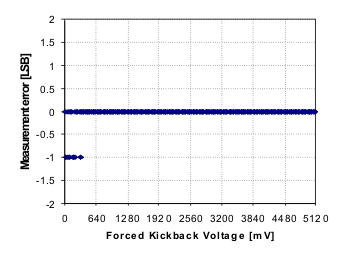
TPS65185 TPS651851 kickback_error_lvsaq8.gif
VIN = 3.7 V
Figure 17. Kickback Voltage Measurement Error
TPS65185 TPS651851 kickback_timing2_lvsaq8.gif
VIN = 3.7 V AVG[1:0] = 11 (Eight Measurements)
Time from ACQ Bit Set to ACQC Interrupt Received
Figure 19. Kickback Voltage Measurement Timing
TPS65185 TPS651851 dflt_pwrdwn_lvsaq8.gif
Figure 4. Default Power-Down Sequence
TPS65185 TPS651851 inrush_5v_lvsaq8.gif
VIN = 5 V CIN = 100 µF
Figure 6. Inrush Current
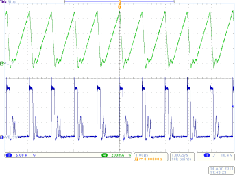
TPS65185 TPS651851 switching_vb_lvsaq8.gif
VIN = 3 V RLOAD, VPOS = 330 Ω RLOAD, VNEG = 330 Ω
No Load on VDDH, VEE
Figure 8. Switching Waveforms, VB
TPS65185 TPS651851 switching_vb2_lvsaq8.gif
VIN = 3.7 V RLOAD, VPOS = 330 Ω RLOAD, VNEG = 330 Ω
No Load on VDDH, VEE
Figure 10. Switching Waveforms, VB
TPS65185 TPS651851 switching_vb3_lvsaq8.gif
VIN = 5 V RLOAD, VPOS = 330 Ω RLOAD, VNEG = 330 Ω
No Load on VDDH, VEE
Figure 12. Switching Waveforms, VB
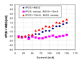
TPS65185 TPS651851 src_driver_lvsaq8.gif
VIN = 3.7 V
Figure 14. Source Driver Supply Tracking
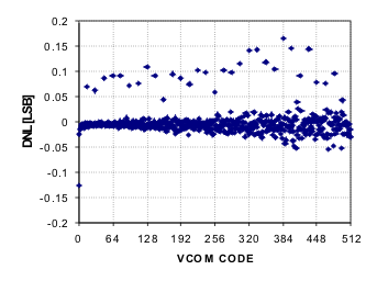
TPS65185 TPS651851 vcom_diff_nonlin_lvsaq8.gif
VIN = 3.7 V RLOAD, VCOM = 1 kΩ
Figure 16. VCOM Differential Non-Linearity
TPS65185 TPS651851 kickback_timing1_lvsaq8.gif
VIN = 3.7 V AVG[1:0] = 00 (Single Measurement)
Time from ACQ Bit Set to ACQC Interrupt Received
Figure 18. Kickback Voltage Measurement Timing