ZHCSLR2C August   2020  – March 2022 TPS61288

PRODUCTION DATA  

  1. 特性
  2. 应用
  3. 说明
  4. Revision History
  5. Device Comparison
  6. Pin Configuration and Functions
  7. Specifications
    1. 7.1 Absolute Maximum Ratings
    2. 7.2 ESD Ratings
    3. 7.3 Recommended Operating Conditions
    4. 7.4 Thermal Information
    5. 7.5 Electrical Characteristics
    6. 7.6 Typical Characteristics
  8. Detailed Description
    1. 8.1 Overview
    2. 8.2 Functional Block Diagram
    3. 8.3 Feature Description
      1. 8.3.1 Enable and Start-up
      2. 8.3.2 Undervoltage Lockout (UVLO)
      3. 8.3.3 Switching Peak Current Limit
      4. 8.3.4 Overvoltage Protection
      5. 8.3.5 Thermal Shutdown
    4. 8.4 Device Functional Modes
      1. 8.4.1 PWM
      2. 8.4.2 PFM
  9. Application and Implementation
    1. 9.1 Application Information
    2. 9.2 Typical Application
      1. 9.2.1 Design Requirements
      2. 9.2.2 Detailed Design Procedure
        1. 9.2.2.1 Setting Output Voltage
        2. 9.2.2.2 Inductor Selection
        3. 9.2.2.3 Input Capacitor Selection
        4. 9.2.2.4 Output Capacitor Selection
        5. 9.2.2.5 Loop Stability
      3. 9.2.3 Application Curves
  10. 10Power Supply Recommendations
  11. 11Layout
    1. 11.1 Layout Guidelines
    2. 11.2 Layout Example
      1. 11.2.1 Thermal Considerations
  12. 12Device and Documentation Support
    1. 12.1 Receiving Notification of Documentation Updates
    2. 12.2 支持资源
    3. 12.3 Trademarks
    4. 12.4 Electrostatic Discharge Caution
    5. 12.5 术语表
  13. 13Mechanical, Packaging, and Orderable Information

封装选项

机械数据 (封装 | 引脚)
散热焊盘机械数据 (封装 | 引脚)
订购信息

Output Capacitor Selection

For small output voltage ripple, TI recommends a low-ESR output capacitor like a ceramic capacitor. Typically, three 22-μF ceramic output capacitors work for most applications. Higher capacitor values can be used to improve the load transient response. Take care when evaluating the derating of the capacitor under DC bias. The bias can significantly reduce capacitance. Ceramic capacitors can lose most of their capacitance at rated voltage. Therefore, leave margin on the voltage rating to ensure adequate effective capacitance. From the required output voltage ripple, use the following equations to calculate the minimum required effective capacitance COUT:
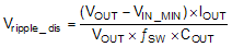
Equation 5. GUID-E116B616-090F-4A34-A622-04CF67C1A4CA-low.gif
Equation 6. GUID-38A80B61-0E33-41D5-9D55-92B738F57B37-low.gif

where

  • Vripple_dis is output voltage ripple caused by charging and discharging of the output capacitor.
  • Vripple_ESR is output voltage ripple caused by ESR of the output capacitor.
  • VIN_MIN is the minimum input voltage of boost converter.
  • VOUT is the output voltage.
  • IOUT is the output current.
  • ILpeak is the peak current of the inductor.
  • ƒSW is the converter switching frequency.
  • RC_ESR is the ESR of the output capacitors.