ZHCS979G June 2012 – November 2025 TPS53318 , TPS53319
PRODUCTION DATA
7.3.7 电流检测、过流和短路保护
TPS53318 和 TPS53319 器件提供逐周期过流限制控制。在关断状态期间会监测电感器电流,而控制器会在电感器电流大于过流跳变电平期间保持关断状态。为了实现良好的精度和经济高效的设计,TPS53319 器件支持温度补偿 MOSFET RDS(on) 检测。TRIP 引脚必须通过跳变电压设置电阻器 RTRIP 连接到 GND。TRIP 端子提供电流 (ITRIP),该电流在室温下的典型值为 10μA,跳变电平则设置为 OCL 跳变电压 VTRIP,如方程式 2 所示。

电感器电流由 LL 引脚监测。GND 引脚用作正电流检测节点,LL 引脚用作负电流检测节点。跳变电流 ITRIP 具有 3000ppm/°C 的温度斜率,以补偿 RDS(on) 对温度的依赖性。对于每个器件,还会根据生产测试中特定于器件的导通电阻测量值来调整 ITRIP,以消除不同器件之间的任何 OCP 变化。占空比不得超过 45%,以提供更准确的 OCP。
由于在关断状态下进行比较,所以 VTRIP 将设置电感器电流的谷值电平。因此,过流阈值 IOCP 下的负载电流可按方程式 3 所示进行计算。

其中
- RTRIP 的单位为 Ω
在过流或短路情况下,流向负载的电流超过流向输出电容器的电流,因此输出电压趋于下降。最终,它会跨过欠压保护阈值并关断。经过断续延迟(16ms 加 0.7ms 软启动周期)后,控制器将重新启动。如果过流条件仍然存在,则重复该过程,且器件进入断续模式。
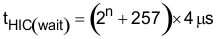
其中
- n = 8、9、10 或 11,具体取决于软启动时间选择
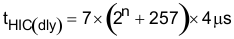
| 选择的软启动时间 (tSS) (ms) | 断续等待时间 (tHIC(wait)) (ms) | 断续延迟时间 (tHIC(delay)) (ms) |
|---|---|---|
| 0.7 | 2.052 | 14.364 |
| 1.4 | 3.076 | 21.532 |
| 2.8 | 5.124 | 35.868 |
| 5.6 | 9.220 | 64.540 |
对于 TPS53318 器件,OCP 阈值在内部钳位至 10.5A。TPS53318 器件的建议 RTRIP 值小于 150kΩ。