ZHCS979G June 2012 – November 2025 TPS53318 , TPS53319
PRODUCTION DATA
7.3.13 采用全陶瓷输出电容器的外部元件选择
当使用陶瓷输出电容器时,无法满足方程式 7 中的稳定性标准。实现图 8-1 所示的纹波注入方法,以增加 VFB 引脚上的纹波并使系统稳定。除了使用节 8.2.1.2中的步骤 1 至步骤 6 进行的选择外,还必须选择纹波注入元件。C2 值可固定为 1nF。C1 的值可以在 10nF 至 200nF 之间进行选择。
其中
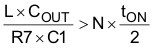
- N 是考虑 L 和 COUT 变化的系数
N 还用于提供足够的裕度以确保稳定性。TI 建议在 VOUT ≤ 1.8V 时选择 N = 2,在 VOUT ≥ 3.3V 或 L ≤ 250nH 时选择 N = 4。VOUT 越高,需要的 N 值也越高,这是因为有效输出电容会随着直流偏置电压的升高而显著降低。例如,6.3V、22µF 陶瓷电容器在偏置为 5V 时的有效电容只有 8µF。
由于 VFB 引脚电压稳压在谷值,所以 VFB 引脚上的纹波增加会导致 VFB 直流值增加。耦合到 VFB 引脚的交流纹波有两个分量,一个从 SW 节点耦合,另一个从 VOUT 引脚耦合;在忽略等效串联电感 (ESL) 引起的输出电压纹波时,可以使用方程式 9 和方程式 10 来计算这些分量的值。
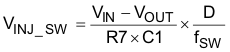

TI 建议使 VINJ_SW 小于 50mV。如果计算得出的 VINJ_SW 大于 50mV,则需要调整其他参数来降低 VINJ_SW。例如,可以增加 COUT 并选择更高的 R7 值以满足方程式 8,从而降低 VINJ_SW。
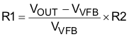
VFB 引脚上的直流电压可通过方程式 11 计算得出:

电阻分压器的值可通过方程式 12 确定: