ZHCSF29E May 2016 – January 2021 TPS25940-Q1
PRODMIX
- 1 特性
- 2 应用
- 3 说明
- 4 Revision History
- 5 Device Comparison Table
- 6 Pin Configuration and Functions
- 7 Specifications
- 8 Parametric Measurement Information
-
9 Detailed Description
- 9.1 Overview
- 9.2 Functional Block Diagram
- 9.3 Feature Description
- 9.4 Device Functional Modes
-
10Application and Implementation
- 10.1 Application Information
- 10.2
Typical Application
- 10.2.1 Design Requirements
- 10.2.2
Detailed Design Procedure
- 10.2.2.1 Step by Step Design Procedure
- 10.2.2.2 Programming the Current-Limit Threshold: R(ILIM) Selection
- 10.2.2.3 Undervoltage Lockout and Overvoltage Set Point
- 10.2.2.4 Programming Current Monitoring Resistor—RIMON
- 10.2.2.5 Setting Output Voltage Ramp Time (tdVdT)
- 10.2.2.6 Programing the Power Good Set Point
- 10.2.2.7 Support Component Selections—R6, R7 and CIN
- 10.2.3 Application Curves
- 10.2.4 System Examples
- 11Power Supply Recommendations
- 12Layout
- 13Device and Documentation Support
- 14Mechanical, Packaging, and Orderable Information
9.3.3 Hot Plug-In and In-Rush Current Control
The device is designed to control the in-rush current upon insertion of a card into a live backplane or other "hot" power source. This limits the voltage sag on the backplane’s supply voltage and prevents unintended resets of the system power. A slew rate controlled startup (dVdT) also helps to eliminate conductive and radiative interferences. An external capacitor connected from the dVdT pin to GND defines the slew rate of the output voltage at power-on (as shown in Figure 9-2). Equation governing slew rate at start-up is shown in Equation 1.
") Figure 9-2 Output Ramp Up Time tdVdT is Set by C(dVdT)
Figure 9-2 Output Ramp Up Time tdVdT is Set by C(dVdT)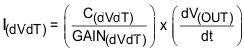
where
- I(dVdT) = 1 µA (typical)
-
 = Desired output slew rate
 - GAIN(dVdT) = dVdT to OUT gain = 12
The total ramp time (tdVdT) of V(OUT) for 0 to V(IN) can be calculated using Equation 2.
The inrush current, I(INRUSH) can be calculated as shown in Equation 3.
The dVdT pin can be left floating to obtain a predetermined slew rate (tdVdT) on the output. When terminal is left floating, the device sets an internal ramp rate of 30 V/ms for output (V(OUT)) ramp.
Figure 10-7 and Figure 10-8 illustrate the inrush current control behavior of the device. For systems where load is present during start-up, the current never exceeds the overcurrent limit set by R(ILIM) resistor for the application. For defining appropriate charging time-rate under different load conditions, see the Setting Output Voltage Ramp Time (TdVdT) section.