ZHCSF29E May 2016 – January 2021 TPS25940-Q1
PRODMIX
- 1 特性
- 2 应用
- 3 说明
- 4 Revision History
- 5 Device Comparison Table
- 6 Pin Configuration and Functions
- 7 Specifications
- 8 Parametric Measurement Information
-
9 Detailed Description
- 9.1 Overview
- 9.2 Functional Block Diagram
- 9.3 Feature Description
- 9.4 Device Functional Modes
-
10Application and Implementation
- 10.1 Application Information
- 10.2
Typical Application
- 10.2.1 Design Requirements
- 10.2.2
Detailed Design Procedure
- 10.2.2.1 Step by Step Design Procedure
- 10.2.2.2 Programming the Current-Limit Threshold: R(ILIM) Selection
- 10.2.2.3 Undervoltage Lockout and Overvoltage Set Point
- 10.2.2.4 Programming Current Monitoring Resistor—RIMON
- 10.2.2.5 Setting Output Voltage Ramp Time (tdVdT)
- 10.2.2.6 Programing the Power Good Set Point
- 10.2.2.7 Support Component Selections—R6, R7 and CIN
- 10.2.3 Application Curves
- 10.2.4 System Examples
- 11Power Supply Recommendations
- 12Layout
- 13Device and Documentation Support
- 14Mechanical, Packaging, and Orderable Information
10.2.2.4 Programming Current Monitoring Resistor—RIMON
Voltage at IMON pin V(IMON) represents the voltage proportional to load current. This can be connected to an ADC of the downstream system for health monitoring of the system. The R(IMON) need to be configured based on the maximum input voltage range of the ADC used. R(IMON) is set using Equation 13.
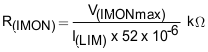
For I(LIM) = 5 A, and considering the operating range of ADC from 0 V to 5 V, V(IMONmax) is 5 V and R(IMON) is determined by:
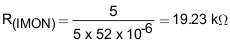
Selecting R(IMON) value less than determined by Equation 14 ensures that ADC limits are not exceeded for maximum value of load current.
If the IMON pin voltage is not being digitized with an ADC, R(IMON) can be selected to produce a 1V/1A voltage at the IMON pin, using Equation 13.
Choose closest 1 % standard value: 19.1 kΩ.
If current monitoring up to I(FASTRIP) is desired, R(IMON) can be reduced by a factor of 1.6, as in Equation 5.