ZHCSF29E May 2016 – January 2021 TPS25940-Q1
PRODMIX
- 1 特性
- 2 应用
- 3 说明
- 4 Revision History
- 5 Device Comparison Table
- 6 Pin Configuration and Functions
- 7 Specifications
- 8 Parametric Measurement Information
-
9 Detailed Description
- 9.1 Overview
- 9.2 Functional Block Diagram
- 9.3 Feature Description
- 9.4 Device Functional Modes
-
10Application and Implementation
- 10.1 Application Information
- 10.2
Typical Application
- 10.2.1 Design Requirements
- 10.2.2
Detailed Design Procedure
- 10.2.2.1 Step by Step Design Procedure
- 10.2.2.2 Programming the Current-Limit Threshold: R(ILIM) Selection
- 10.2.2.3 Undervoltage Lockout and Overvoltage Set Point
- 10.2.2.4 Programming Current Monitoring Resistor—RIMON
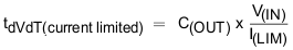
- 10.2.2.5 Setting Output Voltage Ramp Time (tdVdT)
- 10.2.2.6 Programing the Power Good Set Point
- 10.2.2.7 Support Component Selections—R6, R7 and CIN
- 10.2.3 Application Curves
- 10.2.4 System Examples
- 11Power Supply Recommendations
- 12Layout
- 13Device and Documentation Support
- 14Mechanical, Packaging, and Orderable Information
10.2.2.5.2 Case 2: Start-Up With Load: Output Capacitance C(OUT) and Load Draws Current During Start-Up
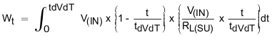
When load draws current during the turn-on sequence, there is additional power dissipated. Considering a resistive load RL(SU) during start-up, load current ramps up proportionally with increase in output voltage during tdVdT time. Typical ramp-up of output voltage, Load current and power dissipation in the device is shown in Figure 10-4 and power dissipation with respect to time is plotted in Figure 10-5. The additional power dissipation during start-up phase is calculated as shown in Equation 17 and Equation 18.
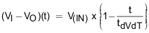
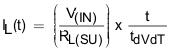
Where RL(SU) is the load resistance present during start-up. Average energy loss in the internal FET during charging time due to resistive load is given by Equation 19.

| V(IN) = 12 V | C(dVdT) = 1 nF | RL(SU) = 4.8 Ω |
 in Load During Start-Up")
| V(IN) = 12 V | C(dVdT) = 1 nF | RL(SU) = 4.8 Ω |
On solving Equation 19 the average power loss in the internal FET due to load is shown in Equation 20.
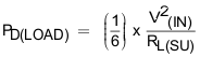
Total power dissipated in the device during startup is shown is Equation 21.

Total current during startup is given by Equation 22.
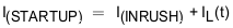
If I(STARTUP) > I(LIM), the device limits the current to I(LIM) and the current limited charging time is determined by Equation 23.
The power dissipation, with and without load, for selected start-up time must not exceed the shutdown limits as shown in Figure 10-6.

For the design example under discussion,
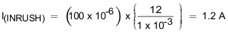
Select ramp-up capacitor C(dVdT) = 1nF, using Equation 24.

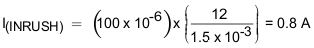
The inrush current drawn by the load capacitance (C(OUT)) during ramp-up using Equation 25.
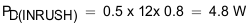
The inrush Power dissipation is calculated, using Equation 26.
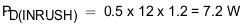
For 7.2 W of power loss, the thermal shut down time of the device must not be less than the ramp-up time tdVdT to avoid the false trip at maximum operating temperature. From thermal shutdown limit graph Figure 10-6 at TA = 85°C, for 7.2 W of power the shutdown time is approximately 60 ms. So it is safe to use 1 ms as start-up time without any load on output.
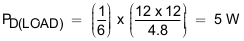
Considering the start-up with load 4.8 Ω, the additional power dissipation, when load is present during start up is calculated, using Equation 27.
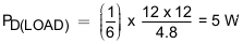
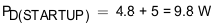
The total device power dissipation during start up is given by Equation 28.
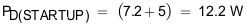
From thermal shutdown limit graph at TA = 85°C, the thermal shutdown time for 12.2 W is close to 7.5 ms. It is safe to have 30% margin to allow for variation of system parameters such as load, component tolerance, and input voltage. So it is well within acceptable limits to use the 1 nF capacitor with start-up load of 4.8 Ω.
If there is a need to decrease the power loss during start-up, it can be done with increase of C(dVdT) capacitor.
To illustrate, choose C(dVdT) = 1.5 nF as an option and recalculate:

From thermal shutdown limit graph at TA = 85°C, the shutdown time for 10-W power dissipation is approximately 17 ms, which increases the margins further for shutdown time and ensures successful operation during start up and steady state conditions.
The spreadsheet tool available on the web can be used for iterative calculations.