ZHCSF29E May   2016  – January 2021 TPS25940-Q1

PRODMIX  

  1. 特性
  2. 应用
  3. 说明
  4. Revision History
  5. Device Comparison Table
  6. Pin Configuration and Functions
  7. Specifications
    1. 7.1 Absolute Maximum Ratings
    2. 7.2 ESD Ratings
    3. 7.3 Recommended Operating Conditions
    4. 7.4 Thermal Information
    5. 7.5 Electrical Characteristics
    6. 7.6 Timing Requirements
    7. 7.7 Typical Characteristics
  8. Parametric Measurement Information
  9. Detailed Description
    1. 9.1 Overview
    2. 9.2 Functional Block Diagram
    3. 9.3 Feature Description
      1. 9.3.1 Enable and Adjusting Undervoltage Lockout
      2. 9.3.2 Overvoltage Protection (OVP)
      3. 9.3.3 Hot Plug-In and In-Rush Current Control
      4. 9.3.4 Overload and Short Circuit Protection
        1. 9.3.4.1 Overload Protection
        2. 9.3.4.2 Short Circuit Protection
        3. 9.3.4.3 Start-Up with Short on Output
        4. 9.3.4.4 Constant Current Limit Behavior During Overcurrent Faults
      5. 9.3.5 FAULT Response
      6. 9.3.6 Current Monitoring
      7. 9.3.7 Power Good Comparator
      8. 9.3.8 IN, OUT and GND Pins
      9. 9.3.9 Thermal Shutdown
    4. 9.4 Device Functional Modes
      1. 9.4.1 DevSleep Mode
      2. 9.4.2 Shutdown Control
  10. 10Application and Implementation
    1. 10.1 Application Information
    2. 10.2 Typical Application
      1. 10.2.1 Design Requirements
      2. 10.2.2 Detailed Design Procedure
        1. 10.2.2.1 Step by Step Design Procedure
        2. 10.2.2.2 Programming the Current-Limit Threshold: R(ILIM) Selection
        3. 10.2.2.3 Undervoltage Lockout and Overvoltage Set Point
        4. 10.2.2.4 Programming Current Monitoring Resistor—RIMON
        5. 10.2.2.5 Setting Output Voltage Ramp Time (tdVdT)
          1. 10.2.2.5.1 Case1: Start-Up Without Load: Only Output Capacitance C(OUT) Draws Current During Start-Up
          2. 10.2.2.5.2 Case 2: Start-Up With Load: Output Capacitance C(OUT) and Load Draws Current During Start-Up
        6. 10.2.2.6 Programing the Power Good Set Point
        7. 10.2.2.7 Support Component Selections—R6, R7 and CIN
      3. 10.2.3 Application Curves
      4. 10.2.4 System Examples
        1. 10.2.4.1 VBUS Short-to-Battery, Short-to-Ground Protection of USB Port in Automotive Systems
        2. 10.2.4.2 Power Failure Protection for Holdup Power
        3. 10.2.4.3 Overload Detection Using TPS25940xx-Q1
  11. 11Power Supply Recommendations
    1. 11.1 Transient Protection
    2. 11.2 Output Short-Circuit Measurements
  12. 12Layout
    1. 12.1 Layout Guidelines
    2. 12.2 Layout Example
  13. 13Device and Documentation Support
    1. 13.1 Documentation Support
      1. 13.1.1 Related Documentation
    2. 13.2 支持资源
    3. 13.3 Trademarks
    4. 13.4 静电放电警告
    5. 13.5 术语表
  14. 14Mechanical, Packaging, and Orderable Information

封装选项

机械数据 (封装 | 引脚)
散热焊盘机械数据 (封装 | 引脚)
订购信息

IN, OUT and GND Pins

The device has multiple pins for input (IN) and output (OUT).

All IN pins must be connected together and to the power source. A ceramic bypass capacitor close to the device from IN to GND is recommended to alleviate bus transients. The recommended operating voltage range is
2.7 V – 18 V.

Similarly all OUT pins must be connected together and to the load. V(OUT) in the ON condition, is calculated using Equation 8.

Equation 8. GUID-0E4C3EBF-4A33-4959-A2FC-27ED4D0356DA-low.gif

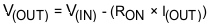
where, RON is the total ON resistance of the internal FET.

GND terminal is the most negative voltage in the circuit and is used as a reference for all voltage reference unless otherwise specified.