ZHCSF29E May   2016  – January 2021 TPS25940-Q1

PRODMIX  

  1. 特性
  2. 应用
  3. 说明
  4. Revision History
  5. Device Comparison Table
  6. Pin Configuration and Functions
  7. Specifications
    1. 7.1 Absolute Maximum Ratings
    2. 7.2 ESD Ratings
    3. 7.3 Recommended Operating Conditions
    4. 7.4 Thermal Information
    5. 7.5 Electrical Characteristics
    6. 7.6 Timing Requirements
    7. 7.7 Typical Characteristics
  8. Parametric Measurement Information
  9. Detailed Description
    1. 9.1 Overview
    2. 9.2 Functional Block Diagram
    3. 9.3 Feature Description
      1. 9.3.1 Enable and Adjusting Undervoltage Lockout
      2. 9.3.2 Overvoltage Protection (OVP)
      3. 9.3.3 Hot Plug-In and In-Rush Current Control
      4. 9.3.4 Overload and Short Circuit Protection
        1. 9.3.4.1 Overload Protection
        2. 9.3.4.2 Short Circuit Protection
        3. 9.3.4.3 Start-Up with Short on Output
        4. 9.3.4.4 Constant Current Limit Behavior During Overcurrent Faults
      5. 9.3.5 FAULT Response
      6. 9.3.6 Current Monitoring
      7. 9.3.7 Power Good Comparator
      8. 9.3.8 IN, OUT and GND Pins
      9. 9.3.9 Thermal Shutdown
    4. 9.4 Device Functional Modes
      1. 9.4.1 DevSleep Mode
      2. 9.4.2 Shutdown Control
  10. 10Application and Implementation
    1. 10.1 Application Information
    2. 10.2 Typical Application
      1. 10.2.1 Design Requirements
      2. 10.2.2 Detailed Design Procedure
        1. 10.2.2.1 Step by Step Design Procedure
        2. 10.2.2.2 Programming the Current-Limit Threshold: R(ILIM) Selection
        3. 10.2.2.3 Undervoltage Lockout and Overvoltage Set Point
        4. 10.2.2.4 Programming Current Monitoring Resistor—RIMON
        5. 10.2.2.5 Setting Output Voltage Ramp Time (tdVdT)
          1. 10.2.2.5.1 Case1: Start-Up Without Load: Only Output Capacitance C(OUT) Draws Current During Start-Up
          2. 10.2.2.5.2 Case 2: Start-Up With Load: Output Capacitance C(OUT) and Load Draws Current During Start-Up
        6. 10.2.2.6 Programing the Power Good Set Point
        7. 10.2.2.7 Support Component Selections—R6, R7 and CIN
      3. 10.2.3 Application Curves
      4. 10.2.4 System Examples
        1. 10.2.4.1 VBUS Short-to-Battery, Short-to-Ground Protection of USB Port in Automotive Systems
        2. 10.2.4.2 Power Failure Protection for Holdup Power
        3. 10.2.4.3 Overload Detection Using TPS25940xx-Q1
  11. 11Power Supply Recommendations
    1. 11.1 Transient Protection
    2. 11.2 Output Short-Circuit Measurements
  12. 12Layout
    1. 12.1 Layout Guidelines
    2. 12.2 Layout Example
  13. 13Device and Documentation Support
    1. 13.1 Documentation Support
      1. 13.1.1 Related Documentation
    2. 13.2 支持资源
    3. 13.3 Trademarks
    4. 13.4 静电放电警告
    5. 13.5 术语表
  14. 14Mechanical, Packaging, and Orderable Information

封装选项

机械数据 (封装 | 引脚)
散热焊盘机械数据 (封装 | 引脚)
订购信息
Case1: Start-Up Without Load: Only Output Capacitance C(OUT) Draws Current During Start-Up

During start-up, as the output capacitor charges, the voltage difference across the internal FET decreases, and the power dissipated decreases as well. Typical ramp-up of output voltage V(OUT) with inrush current limit of 1.2 A and power dissipated in the device during start-up is shown in Figure 10-2. The average power dissipated in the device during start-up is equal to area of triangular plot (red curve in Figure 10-2) averaged over tdVdT.

GUID-5D2316CD-B093-4872-BE6D-4EE096820534-low.png
V(IN) = 12 VC(dVdT) = 1 nFC(OUT)=100 µF
Figure 10-2 Start-Up Without Load
GUID-C23E8DB8-E0DE-4ECC-962A-24EA53E39FCD-low.png
V(IN) = 12 V C(dVdT) = 1 nF C(OUT)=100 µF
Figure 10-3 PD(INRUSH) Due to Inrush Current

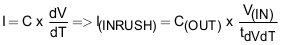
For the TPS25940-Q1 device, the inrush current is determined as shown in Equation 15.

Equation 15. GUID-D2B4009A-0413-4864-AD91-04A78C4602B6-low.gif

Power dissipation during start-up is given by Equation 16.

Equation 16. GUID-BF668BE4-5A70-4886-A725-2E348981AEAC-low.gif

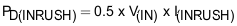
Equation 16 assumes that load does not draw any current until the output voltage has reached its final value.