ZHCS020J January 2011 – March 2021 OPA2835 , OPA835
PRODUCTION DATA
- 1 特性
- 2 应用
- 3 说明
- 4 Revision History
- 5 Device Comparision Table
- 6 Pin Configuration and Functions
-
7 Specifications
- 7.1 Absolute Maximum Ratings
- 7.2 ESD Ratings
- 7.3 Recommended Operating Conditions
- 7.4 Thermal Information: OPA835
- 7.5 Thermal Information: OPA2835
- 7.6 Electrical Characteristics: VS = 2.7 V
- 7.7 Electrical Characteristics: VS = 5 V
- 7.8 Typical Characteristics: VS = 2.7 V
- 7.9 Typical Characteristics: VS = 5 V
- 8 Detailed Description
-
9 Application and Implementation
- 9.1
Application Information
- 9.1.1 Noninverting Amplifier
- 9.1.2 Inverting Amplifier
- 9.1.3 Instrumentation Amplifier
- 9.1.4 Attenuators
- 9.1.5 Single-Ended to Differential Amplifier
- 9.1.6 Differential to Single-Ended Amplifier
- 9.1.7 Differential-to-Differential Amplifier
- 9.1.8 Gain Setting With OPA835 RUN Integrated Resistors
- 9.1.9 Pulse Application With Single-Supply
- 9.1.10 ADC Driver Performance
- 9.2 Typical Application
- 9.1
Application Information
- 10Power Supply Recommendations
- 11Layout
- 12Device and Documentation Support
- 13Mechanical, Packaging, and Orderable Information
封装选项
机械数据 (封装 | 引脚)
散热焊盘机械数据 (封装 | 引脚)
- RUN|10
订购信息
8.3.4 Low-Power Applications and the Effects of Resistor Values on Bandwidth
The OPA835 and OPA2835 devices are designed for the nominal value of RF to be 2 kΩ in gains other than +1. This gives excellent distortion performance, maximum bandwidth, best flatness, and best pulse response. It also loads the amplifier. For example; in gain of 2 with RF = RG = 2 kΩ, RG to ground, and VOUT = 4 V, 1 mA of current will flow through the feedback path to ground. In gain of +1, RG is open and no current will flow to ground. In low-power applications, it is desirable to reduce the current in the feedback path by increasing the gain-setting resistors values. Using larger value gain resistors has two primary side effects (other than lower power) due to their interaction with parasitic circuit capacitance.
- Lowers the bandwidth
- Lowers the phase margin
- This causes peaking in the frequency response
- This causes overshoot and ringing in the pulse response
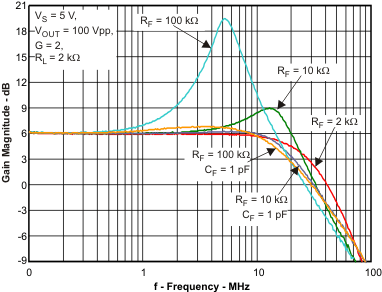
Figure 8-3 shows the small-signal frequency response on OPA835EVM for noninverting gain of 2 with RF and RG equal to 2 kΩ, 10 kΩ, and 100 kΩ. The test was done with RL = 2 kΩ. Due to loading effects of RL, lower RL values may reduce the peaking, but higher values will not have a significant effect.
 Figure 8-3 Frequency Response With Various Gain-Setting Resistor Values
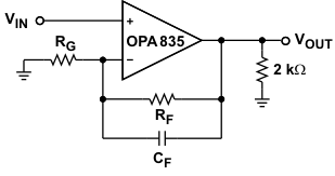
As expected, larger value gain resistors cause lower bandwidth and peaking in the response (peaking in frequency response is synonymous with overshoot and ringing in pulse response). Adding 1-pF capacitors in parallel with RF helps compensate the phase margin and restores flat frequency response. Figure 8-4 shows the test circuit.
 Figure 8-4 G = 2
Test Circuit for Various Gain-Setting Resistor Values