ZHCS020J January 2011 – March 2021 OPA2835 , OPA835
PRODUCTION DATA
- 1 特性
- 2 应用
- 3 说明
- 4 Revision History
- 5 Device Comparision Table
- 6 Pin Configuration and Functions
-
7 Specifications
- 7.1 Absolute Maximum Ratings
- 7.2 ESD Ratings
- 7.3 Recommended Operating Conditions
- 7.4 Thermal Information: OPA835
- 7.5 Thermal Information: OPA2835
- 7.6 Electrical Characteristics: VS = 2.7 V
- 7.7 Electrical Characteristics: VS = 5 V
- 7.8 Typical Characteristics: VS = 2.7 V
- 7.9 Typical Characteristics: VS = 5 V
- 8 Detailed Description
-
9 Application and Implementation
- 9.1
Application Information
- 9.1.1 Noninverting Amplifier
- 9.1.2 Inverting Amplifier
- 9.1.3 Instrumentation Amplifier
- 9.1.4 Attenuators
- 9.1.5 Single-Ended to Differential Amplifier
- 9.1.6 Differential to Single-Ended Amplifier
- 9.1.7 Differential-to-Differential Amplifier
- 9.1.8 Gain Setting With OPA835 RUN Integrated Resistors
- 9.1.9 Pulse Application With Single-Supply
- 9.1.10 ADC Driver Performance
- 9.2 Typical Application
- 9.1
Application Information
- 10Power Supply Recommendations
- 11Layout
- 12Device and Documentation Support
- 13Mechanical, Packaging, and Orderable Information
封装选项
机械数据 (封装 | 引脚)
散热焊盘机械数据 (封装 | 引脚)
- RUN|10
订购信息
8.4.2 Single-Supply Operation (2.5 V to 5.5 V)
Often, newer systems use a single power supply to improve efficiency and reduce the cost of the power supply. OPA835 and OPA2835 devices are designed for use with single-supply power operation and can be used with single-supply power with no change in performance from split supply, as long as the input and output are biased within the linear operation of the device.
To change the circuit from split supply to single-supply, level shift all voltages by ½ the difference between the power supply rails. For example, changing from ± 2.5-V split supply to 5-V single-supply is shown in Figure 8-7.
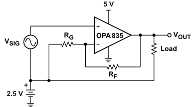 Figure 8-7 Single-Supply Concept
A practical circuit will have an amplifier or other circuit providing the bias voltage for the input, and the output of this amplifier stage provides the bias for the next stage.
Figure 8-8 shows a typical noninverting amplifier circuit. With 5-V single-supply, a mid-supply reference generator is needed to bias the negative side through RG. To cancel the voltage offset that would otherwise be caused by the input bias currents, R1 is selected to be equal to RF in parallel with RG. For example if gain of 2 is required and RF = 2 kΩ, select RG = 2 kΩ to set the gain, and R1 = 1 kΩ for bias current cancellation. The value for C is dependent on the reference, and TI recommends a value of at least 0.1 µF to limit noise.
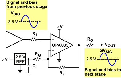 Figure 8-8 Noninverting Single Supply With Reference
Figure 8-9 shows a similar noninverting single-supply scenario with the reference generator replaced by the Thevenin equivalent using resistors and the positive supply. RG’ and RG” form a resistor divider from the 5-V supply and are used to bias the negative side with the parallel sum equal to the equivalent RG to set the gain. To cancel the voltage offset that would otherwise be caused by the input bias currents, R1 is selected to be equal to RF in parallel with RG’ in parallel with RG” (R1= RF || RG’ || RG”). For example, if a gain of 2 is required and RF = 2 kΩ, selecting RG’ = RG” = 4 kΩ gives equivalent parallel sum of 2 kΩ, sets the gain to 2, and references the input to mid supply (2.5 V). R1 is set to 1 kΩ for bias current cancellation. The resistor divider costs less than the 2.5V reference in Figure 8-8 but may increase the current from the 5-V supply.
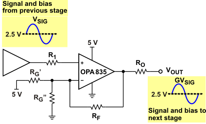 Figure 8-9 Noninverting Single Supply With Resistors
Figure 8-10 shows a typical inverting-amplifier circuit. With a 5-V single-supply, a mid-supply reference generator is needed to bias the positive side through R1. To cancel the voltage offset that would otherwise be caused by the input bias currents, R1 is selected to be equal to RF in parallel with RG. For example, if a gain of –2 is required and RF = 2 kΩ, select RG = 1 kΩ to set the gain and R1 = 667 Ω for bias current cancellation. The value for C is dependent on the reference, but TI recommends a value of at least 0.1 µF to limit noise into the op amp.
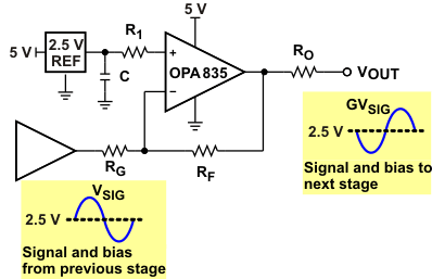 Figure 8-10 Inverting Single Supply With Reference
Figure 8-11 shows a similar inverting single-supply scenario with the reference generator replaced by the Thevenin equivalent using resistors and the positive supply. R1 and R2 form a resistor divider from the 5-V supply and are used to bias the positive side. To cancel the voltage offset that would otherwise be caused by the input bias currents, set the parallel sum of R1 and R2 equal to the parallel sum of RF and RG. C must be added to limit coupling of noise into the positive input. For example, if gain of –2 is required and RF = 2 kΩ, select RG = 1 kΩ to set the gain. R1 = R2 = 667 Ω for mid-supply voltage bias and for op-amp input-bias current cancellation. A good value for C is 0.1 µF. The resistor divider costs less than the 2.5-V reference in Figure 8-10 but may increase the current from the 5-V supply.
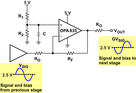 Figure 8-11 Inverting Single Supply With Resistors