ZHCS020J January 2011 – March 2021 OPA2835 , OPA835
PRODUCTION DATA
- 1 特性
- 2 应用
- 3 说明
- 4 Revision History
- 5 Device Comparision Table
- 6 Pin Configuration and Functions
-
7 Specifications
- 7.1 Absolute Maximum Ratings
- 7.2 ESD Ratings
- 7.3 Recommended Operating Conditions
- 7.4 Thermal Information: OPA835
- 7.5 Thermal Information: OPA2835
- 7.6 Electrical Characteristics: VS = 2.7 V
- 7.7 Electrical Characteristics: VS = 5 V
- 7.8 Typical Characteristics: VS = 2.7 V
- 7.9 Typical Characteristics: VS = 5 V
- 8 Detailed Description
-
9 Application and Implementation
- 9.1
Application Information
- 9.1.1 Noninverting Amplifier
- 9.1.2 Inverting Amplifier
- 9.1.3 Instrumentation Amplifier
- 9.1.4 Attenuators
- 9.1.5 Single-Ended to Differential Amplifier
- 9.1.6 Differential to Single-Ended Amplifier
- 9.1.7 Differential-to-Differential Amplifier
- 9.1.8 Gain Setting With OPA835 RUN Integrated Resistors
- 9.1.9 Pulse Application With Single-Supply
- 9.1.10 ADC Driver Performance
- 9.2 Typical Application
- 9.1
Application Information
- 10Power Supply Recommendations
- 11Layout
- 12Device and Documentation Support
- 13Mechanical, Packaging, and Orderable Information
封装选项
机械数据 (封装 | 引脚)
散热焊盘机械数据 (封装 | 引脚)
- RUN|10
订购信息
9.1.6 Differential to Single-Ended Amplifier
Figure 9-4 shows a differential amplifier that converts differential signals to single-ended and provides gain (or attenuation) and level shifting. This circuit can be used in applications like a line receiver for converting a differential signal from a Cat5 cable to a single-ended signal.
If VIN+ = VCM + VSIG+ and VIN– = VCM + VSIG–, then the output of the amplifier may be calculated according to Equation 5.
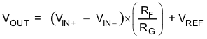
The signal gain of the circuit is
 , VCM is rejected, and VREF provides a level shift around which the output signal swings. The single-ended output signal is in-phase with the differential input signal.
 Figure 9-4 Differential to Single-Ended Amplifier
Line termination can be accomplished by adding a shunt resistor across the VIN+ and VIN- inputs. The differential impedance is the shunt resistance in parallel with the input impedance of the amplifier circuit, which is usually much higher. For low gain and low line impedance, the resistor value to add is approximately the impedance of the line. For example, if a 100-Ω Cat5 cable is used with a gain of 1 amplifier and RF = RG = 2 kΩ, adding a 100-Ω shunt across the input will give a differential impedance of 99 Ω, which is adequate for most applications.
For best CMRR performance, resistors must be matched. Assuming CMRR ≈ the resistor tolerance, a 0.1% tolerance will provide about 60-dB CMRR.